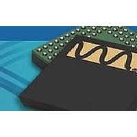
WM9090ECS/R Wolfson Microelectronics, WM9090ECS/R Datasheet - Page 15

WM9090ECS/R
Manufacturer Part Number
WM9090ECS/R
Description
Audio CODECs Audio Subsystem w/ capless headphones
Manufacturer
Wolfson Microelectronics
Specifications of WM9090ECS/R
Interface Type
2-Wire, l2C
Thd Plus Noise
80 dB
Ic Function
Ultra Low Power Audio Subsystem
Brief Features
Mono Class D Speaker Driver, Automatic Gain Control (AGC)
Supply Voltage Range
2.7V To 5.5V
Operating Temperature Range
-40°C To +85°C
Rohs Compliant
Yes
Lead Free Status / RoHS Status
Lead free / RoHS Compliant
w
Pre-Production
LINE INPUTS
All of the analogue input pins are designed as line inputs. These pins can be configured as single-
ended or differential inputs, with flexible routing options and gain controls suitable for many different
usage cases. These inputs provide a high gain path for low input signal levels.
The line input pins IN1P and IN1N provide a differential input path to PGA IN1A. If required, these
input pins can be configured as two separate single-ended inputs to PGAs IN1A and IN1B
respectively. Single ended configuration is selected by writing a 0 to the IN1_DIFF register bit.
The line input pins IN2P and IN2N provide a differential input path to PGA IN2A. If required, these
input pins can be configured as two separate single-ended inputs to PGAs IN2A and IN2B
respectively. Single ended configuration is selected by writing a 0 to the IN2_DIFF register bit.
Signal path configuration to the input PGAs is detailed later in this section. Signal path configuration
to the output mixers and speaker mixers is described in “Output Signal Path”.
Note that, by default, the analogue input pins are clamped to VMID in order to prevent audible pops
caused by enabling the input paths. When one or more analogue input path is in use, the respective
input clamp(s) must be disabled using the register bits described under “Power Sequences and Pop
Suppression Control”.
INPUT PGA ENABLE
The Input PGAs are enabled using register bits IN1A_ENA, IN1B_ENA, IN2A_ENA and IN2B_ENA,
as described in Table 1. The Input PGAs must be enabled for line input on the respective input pins.
Note that, for differential input on IN1P and IN1N, it is not necessary to enable PGA IN1B.
Note that, for differential input on IN2P and IN2N, it is not necessary to enable PGA IN2B.
Table 1 Input PGA Enable
For normal operation of the input PGAs, the reference voltage VMID and the bias current must also
be enabled. See “Reference Voltages and Master Bias” for details of the associated controls
VMID_RES and BIAS_ENA.
R2 (02h)
Power
Management
(2)
REGISTER
ADDRESS
BIT
7
6
5
4
IN1A_ENA
IN1B_ENA
IN2A_ENA
IN2B_ENA
LABEL
DEFAULT
0
0
0
0
IN1A Input PGA Enable
0 = Disabled
1 = Enabled
IN1B Input PGA Enable
0 = Disabled
1 = Enabled
(Note this is only required for single-ended
input on the IN1N pin)
IN2A Input PGA Enable
0 = Disabled
1 = Enabled
IN2B Input PGA Enable
0 = Disabled
1 = Enabled
(Note this is only required for single-ended
input on the IN2N pin)
DESCRIPTION
PP, January 2010, Rev 3.0
WM9090
15


