TGA2521-SM-T/R TriQuint, TGA2521-SM-T/R Datasheet - Page 12
TGA2521-SM-T/R
Manufacturer Part Number
TGA2521-SM-T/R
Description
RF Amplifier 17 - 24 GHz Driver
Manufacturer
TriQuint
Type
Linear Driver Amplifierr
Datasheet
1.TGA2521-SM-TR.pdf
(18 pages)
Specifications of TGA2521-SM-T/R
Mounting Style
SMD/SMT
Operating Frequency
17 GHz to 24 GHz
P1db
23.5 dBm
Noise Figure
5 dB
Operating Supply Voltage
5 V
Supply Current
320 mA
Maximum Power Dissipation
3.9 W
Package / Case
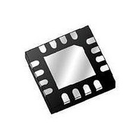
QFN-16
Lead Free Status / RoHS Status
Lead free / RoHS Compliant
Other names
1059496


PIN 1 DOT
BY MARKING
1,2,4,9,10,12
TriQuint Semiconductor: www. triquint.com (972)994-8465 Fax (972)994-8504 Info-mmw@tqs.com
Pin
Pin
6,15
7,13
5,8
11
16
14
17
3
1
2
4
3
1/ Bias network required. See ‘Recommended Application Circuit’ .
16
5
TOP VIEW
15
6
Vd1 (bot), Vd1 (top)
Vd2 (bot), Vd2 (top)
14
7
13
Symbol
Symbol
8
RF Out
RF In
GND
GND
Vg1
Vg2
NC
Package Pinout
12
11
10
9
Feb 2011 © Rev D
Feb 2010 © Rev C
Input, matched to 50 ohms.
Output, matched to 50 ohms.
Gate voltage for amplifier’s input stage. 1/
Gate voltage for amplifier’s 2
Drain voltage for amplifier’s input stage. Must be
biased from both sides. 1/
Drain voltage for amplifier’s 2
Must be biased from both sides. 1/
No internal connection. Must be grounded to the
PCB. See ‘Recommended Land Pattern’.
Connected to 17 internally. Can be grounded or left
open on the PCB.
Backside paddle. Multiple vias on the PCB should
be employed to minimize inductance and thermal
resistance. See ‘Recommended Land Pattern’.
12
11
10
9
BOTTOM VIEW
13
SIDE VIEW
8
14
7
17
15
6
Description
Description
16
5
1
2
3
4
TGA2521-SM
nd
PIN #1 IDENTIFICATION
nd
and final stages. 1/
and final stages.
12
Related parts for TGA2521-SM-T/R
Image
Part Number
Description
Manufacturer
Datasheet
Request
R

Part Number:
Description:
17 - 24 Ghz Linear Driver Amplifier
Manufacturer:
TriQuint Semiconductor
Datasheet:
Part Number:
Description:
17-24 Ghz Linear Driver Amplifier
Manufacturer:
TriQuint Semiconductor
Datasheet:

Part Number:
Description:
Manufacturer:
TriQuint
Datasheet: