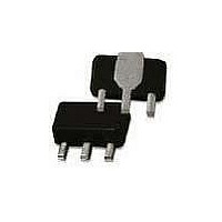
AH125-89PCB900 TriQuint, AH125-89PCB900 Datasheet - Page 8

AH125-89PCB900
Manufacturer Part Number
AH125-89PCB900
Description
RF Modules & Development Tools .4-2.7GHz Eval Board
Manufacturer
TriQuint
Datasheet
1.AH125-89PCB2140.pdf
(12 pages)
Specifications of AH125-89PCB900
Board Size
4.25 mm x 4.6 mm x 1.6 mm
Minimum Frequency
400 MHz
Minimum Operating Temperature
- 40 C
Supply Voltage (min)
5 V
Product
RF Modules
Maximum Frequency
3.6 GHz
Supply Voltage (max)
6 V
Supply Current
170 mA
Maximum Operating Temperature
+ 85 C
For Use With/related Products
AH125
Lead Free Status / RoHS Status
Lead free / RoHS Compliant
Other names
1071315
AH125
½W High Linearity InGaP HBT Amplifier
Frequency
Gain
Input Return Loss
Output Return Loss
ACLR
Pout=+16 dBm
Output P1dB
Output IP3
Pout=+10 dBm/tone, 1MHz spacing
Quiescent Current, Icq
Vcc
TriQuint Semiconductor, Inc • Phone 503-615-9000 • FAX: 503-615-8900 • e-mail: info-sales@tqs.com • Web site: www.TriQuint.com
Typical TD-SCDMA Performance at 25°C
19
18
17
16
15
14
50
45
40
35
30
2010
9
T
LEAD
=+25°C
10
C1
C20
R20
2015
OIP3 vs. Output Power per Tone
2010 MHz
11
Output Power/Tone (dBm)
Gain vs. Frequency
Frequency (MHz)
R1
C10
12
2010 2015 2025 MHz
-49.5
16.3
12.6
+28
+45
8.2
2020
2015 MHz
13
C3
C8
C4
C9
+28.3
16.3
13.1
+45
150
-50
8.1
+5
14
C8
R2
2025
T
1 MHz tone spacing
TD-SCDMA 3 Carrier, PAR = 10 dB @ 0.01% Probability, 1.28 MHz BW
LEAD
2.7 GHz
15
C2
=+25°C
-50.1
16.4
14.4
+28
+45
7.9
2010-2025 MHz Reference Design
16
2030
dBm
dBm
dBc
mA
dB
dB
dB
17
V
320
300
280
260
240
220
200
180
160
140
-10
-15
-20
-25
-5
0
2010
10
Notes:
1.
2.
3.
4.
5.
6.
7.
T
T
LEAD
LEAD
12
=+25°C
=+25°C
The primary RF microstrip line is 50 Ω.
Components shown on the silkscreen but not on the schematic are not used.
0 Ω jumpers can be replaced with copper trace in target application.
The edge of C9 is placed at 120 mil from AH125 RFout pin. (13.4
The edge of C2 is placed 275 mil from the edge of C9. (30.7
The edge of C10 is placed at 60 mil from AH125 RFin pin. (6.7
The edge of R1 is placed next to the edge of C10.
Collector Current vs Output Power
14
2015
16
Output Power (dBm)
Frequency (MHz)
Return Loss
18
S11
2020
20
S22
22
24
2025
26
28
2030
30
-35
-40
-45
-50
-55
-60
-65
32
30
28
26
24
22
20
10
4
T
LEAD
T
=+25°C
LEAD
6
=+25°C
12
ACLR vs. Output Average Power
2010 MHz
Output Power vs. Input Power
Output Power (dBm)
8
o
Input Power (dBm)
@ 2015 MHz)
P1dB=+28.3 dBm
14
o
@ 2015 MHz)
o
2015 MHz
10
@ 2015 MHz)
16
Page 8 of 12 April 2010
12
2025 MHz
18
14
16
20


