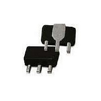
AH125-89PCB900 TriQuint, AH125-89PCB900 Datasheet

RF Modules & Development Tools .4-2.7GHz Eval Board

AH125-89PCB900

Manufacturer Part Number
AH125-89PCB900
Description
RF Modules & Development Tools .4-2.7GHz Eval Board
Manufacturer
TriQuint
Datasheet

Specifications of AH125-89PCB900

Board Size
4.25 mm x 4.6 mm x 1.6 mm
Minimum Frequency
400 MHz
Minimum Operating Temperature
- 40 C
Supply Voltage (min)
5 V
Product
RF Modules
Maximum Frequency
3.6 GHz
Supply Voltage (max)
6 V
Supply Current
170 mA
Maximum Operating Temperature
+ 85 C
For Use With/related Products
AH125
Lead Free Status / RoHS Status
Lead free / RoHS Compliant
Other names
1071315
AH125
½W High Linearity InGaP HBT Amplifier
Product Features
Applications
Specifications
1. Test conditions unless otherwise noted: 25ºC, Vsupply = +5 V, in tuned application circuit.
2. W-CDMA 3GPP Test Model 1+64 DPCH, PAR = 10.3 dB @ 0.01% Probability, 3.84 MHz BW
3. OIP3 is measured with two tones separated by 1 MHz. The suppression on the largest IM3 product
Absolute Maximum Rating
Operation of this device above any of these parameters may cause permanent damage.
TriQuint Semiconductor, Inc • Phone 503-615-9000 • FAX: 503-615-8900 • e-mail: info-sales@tqs.com • Web site: www.TriQuint.com
for 1960 MHz, and 12 dBm/tone for 2140 MHz.
Parameter
Operational Bandwidth
Test Frequency
Gain
Input Return Loss
Output Return Loss
W-CDMA Channel Power
Output P1dB
Output IP3
Noise Figure
Quiescent Collector Current
Device Voltage
Parameter
Storage Temperature
RF Input Power, CW, 50 Ω, T=25°C
Device Voltage
Max Junction Temperature, T
Thermal Resistance, Θ
is used to calculate the OIP3 using a 2:1 rule. Measured at 17dBm/tone for 900 MHz, 14 dBm/tone
400 – 3600 MHz
+28 dBm P1dB
+45 dBm Output IP3
16.2 dB Gain @ 2140 MHz
150 mA current draw
+5 V Single Supply
MTTF > 100 Years
Lead-free/Green/RoHS-compliant
SOT-89 Package
Class 2 HBM ESD rating (>2kV)
Repeaters
Mobile Infrastructure
LTE / WCDMA / EDGE / CDMA
For 10
@ -50 dBc ACLR
6
hours MTTF
(3)
JC
(2)
J
Units Min
MHz
MHz
dBm
dBm
dBm
mA
dB
dB
dB
dB
V
The AH125 is a high dynamic range driver amplifier in a
low-cost surface mount package. The InGaP/GaAs HBT is
able to achieve high performance across a broad range with
+45 dBm OIP3 and +28 dBm of compressed 1dB power
while drawing 150 mA current. The AH125 is available in
a lead-free/green/RoHS-compliant SOT-89 package.
devices are 100% RF and DC tested.
The AH125 is targeted for use as a driver amplifier in
wireless infrastructure where high linearity, medium power,
and high efficiency are required. Internal biasing allows
the AH125 to maintain high linearity over temperature and
operate directly off a single +5V supply. This combination
makes the device an excellent candidate for transceiver line
cards in current and next generation multi-carrier 3G base
stations or repeaters.
Rating
-65 to +150 °C
Input P10dB
+6 V
200 °C
64.3 °C / W
+41
400
130
14
Typ
2140
16.2
+19
+28
+45
150
4.4
Product Description
12
12
+5
Max
3600
170
18
Typical Performance
Ordering Information
Standard T/R size = 1000 pieces on a 7” reel.
Parameter
Frequency
Gain
Input Return Loss
Output Return Loss
W
Output P1dB
Output IP3
Noise Figure
Quiescent Collector Current
Device Voltage
Part No.
AH125-89G
AH125-89PCB900
AH125-89PCB1960
AH125-89PCB2140
AH125-89PCB2600
-
@ -50 dBc ACLR
CDMA Channel Power
(3)
Specifications and information are subject to change without notice
All
Description
½W High Linearity InGaP HBT Amplifier
900 MHz Evaluation Board
1960 MHz Evaluation Board
2140 MHz Evaluation Board
2600 MHz Evaluation Board
(2)
Functional Diagram
Units
MHz
dBm
dBm
dBm
mA
dB
dB
dB
dB
V
RF Output / Vcc
RF IN
1
Function
RF Input
Ground
+28.1
920
+19
+47
9.9
7.7
20
20
GND
GND
2
4
Typical
Page 1 of 12 April 2010
+27.8
1960
+19
+47
150
4.6
+5
17
16
RF OUT
9
Pin No.
3
2, 4
1
3
+28.0
2140
16.2
+19
+45
4.4
12
12

Related parts for AH125-89PCB900

AH125-89PCB900 Summary of contents

Page 1

... Quiescent Collector Current 4.4 Device Voltage 130 150 170 +5 Ordering Information Rating Part No. -65 to +150 °C AH125-89G Input P10dB AH125-89PCB900 +6 V AH125-89PCB1960 200 °C AH125-89PCB2140 64.3 ° AH125-89PCB2600 Standard T/R size = 1000 pieces on a 7” reel. Functional Diagram GND 4 All 1 2 ...

Page 2

... AH125 ½W High Linearity InGaP HBT Amplifier S-Parameters (V Notes: The gain for the unmatched device in 50 ohm system is shown as the trace in black color. For a tuned circuit for a particular frequency expected that actual gain will be higher the maximum stable gain. The maximum stable gain is shown in the dashed red line. ...

Page 3

... The edge of C11 is placed at 40 mil from AH125 RFout pin. (1.7 5. The edge placed at 210 mil from the edge of C11. (8.7 6. The edge placed next to the edge of R3. 7. The edge placed at 100 mil from AH125 RFin pin. (4.2 8. The edge of C10 is placed 250 mil from the edge of R1. (10.4 Return Loss 0 T =+25° ...

Page 4

... AH125 ½W High Linearity InGaP HBT Amplifier 869-960 MHz Reference Design (AH125-89PCB900) W-CDMA 3GPP Test Model 1+64 DPCH, PAR = 10 0.01% Probability, 3.84 MHz BW Typical W-CDMA Performance at 25°C Frequency 869 920 960 Gain Input Return Loss Output Return Loss 10 9.9 9.9 ...

Page 5

... AH125 ½W High Linearity InGaP HBT Amplifier 869-960 MHz Reference Design (AH125-89PCB900) W-CDMA 3GPP Test Model 1+64 DPCH, PAR = 10 0.01% Probability, 3.84 MHz BW Current vs. Output Power 180 T =+25°C LEAD 170 160 150 140 869 MHz 920 MHz 960 MHz 130 ...

Page 6

... The edge placed at 250 mil from AH125 RFout pin. (25.5 5. The edge placed against the edge of C10. 6. The edge of C10 is placed at 30 mil from AH125 RFin pin. (3.1 Return Loss vs. Frequency 0 T =+25°C LEAD -5 ...

Page 7

... The edge placed at 215 mil from AH125 RFout pin. (23.3 5. The edge placed against the edge of C10. 6. The edge of C10 is placed at 80 mil from AH125 RFin pin. (8.7 Input Return Loss vs. Frequency 0 -5 -10 -15 -20 -25 -40° ...

Page 8

... The edge placed at 120 mil from AH125 RFout pin. (13.4 5. The edge placed 275 mil from the edge of C9. (30.7 6. The edge of C10 is placed at 60 mil from AH125 RFin pin. (6.7 7. The edge placed next to the edge of C10. Return Loss 0 T =+25° ...

Page 9

... The edge placed at 120 mils from AH125 RFout pin. (14.2 5. The edge placed at 280 mils from the edge of C9. (33.2 6. The edge of C10 is placed at 60 mils from AH125 RFin pin. (7.1 7. The edge placed 10 mils from the edge of C10. (1.2 Input Return Loss ...

Page 10

... VCC R4 0 Ohms C3 22pF 18nH L1 0805CS Z= 50 Ohm Z= 50 Ohm L=55 mils L=90 mils Ohms 2 C10 C9 0.8pF 0.6pF AH125-89PCB2600 . Ω Return Loss vs. Frequency T =+25°C LEAD S11 S22 2.50 2.60 2.70 2.80 Frequency (GHz) OIP3 vs. Output Power/Tone 2.5 GHz 2.6 GHz 2 ...

Page 11

... Output Power (dBm) Note: This reference design was constructed on FR4 to illustrate potential AH125 performance in the 3.4-3.6 GHz frequency range. For customer applications of AH125 at these frequencies, we recommend the use of more suitable materials such as Rogers 3000 series. TriQuint Semiconductor, Inc • Phone 503-615-9000 • FAX: 503-615-8900 • e-mail: info-sales@tqs.com • Web site: www.TriQuint.com 3 ...

Page 12

... TriQuint Semiconductor, Inc • Phone 503-615-9000 • FAX: 503-615-8900 • e-mail: info-sales@tqs.com • Web site: www.TriQuint.com Mechanical Information Product Marking The AH125 will be marked with an “AH125G” designator with a lot code marked below the part designator. The “Y” represents the last digit of the year the part was manufactured, the “XXX” auto- generated number, and “ ...

Related keywords