LPC-E2468 Olimex Ltd., LPC-E2468 Datasheet
LPC-E2468
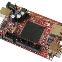
Specifications of LPC-E2468


Related parts for LPC-E2468


LPC-E2468 Summary of contents
Page 1
... LPC-E2468 development board Copyright(c) 2008, OLIMEX Ltd, All rights reserved Rev.B, February 2008 Users Manual ...
Page 2
... FR-4, 1.5 mm, red soldermask, component print; - Dimensions: 90x60mm (3.54 x 2.36"). ELECTROSTATIC WARNING: The LPC-E2468 development board is shipped in protective anti-static packaging. The board must not be subject to high electrostatic potentials. General practice for working with static sensitive devices should be applied when working with this board. ...
Page 3
... AVR-JTAG. You might need other cables in case of other programmers/debuggers. Programmer/debugger AVR-JTAG or any compatible tool. develop projects for the board with Eclipse, IAR, etc. Please, refer to the LPC-E2468 Quickstart Guide which is on the CD for more details on the software requirements SRAM on the ARM local bus for high performance CPU access. ...
Page 4
Four UARTs with fractional baud rate generation, one with ▬ modem control I/O, one with IrDA support, all with FIFO. CAN controller with two channels. ▬ SPI controller. ▬ Two SSP controllers, with FIFO and multi-protocol capabilities. ▬ One is ...
Page 5
On-chip power-on reset. On-chip crystal oscillator with an operating range of 1 MHz to 24 MHz. ● 4 MHz internal RC oscillator trimmed accuracy that can optionally be used as the system clock. When used as ...
Page 6
BLOCK DIAGRAM: ...
Page 7
... MEMORY MAP: LPC2468 memory map ...
Page 8
SCHEMATIC: ...
Page 9
... SRAM and the RTC. The board power consumption is: about 150 mA at 9VDC. RESET CIRCUIT: LPC-E2468 reset circuit is made with RC group R4 – 47K, C20 – 100nF and RESET button. CLOCK CIRCUIT: Quartz crystal 12MHz is connected to LPC2468 pin 44 (XTAL1) and pin 46 (XTAL2) ...
Page 10
JUMPER DESCRIPTION: 3.3V_E VDD1-10 pins of the MCU. 3.3VA_E pin of the VREF_E the VREF pin PHY_PD If the jumper controls the PHY. WP_E the SD/MMC NF_WPE open, disables N_CE/CS1 work through pin of the NAND flash MCU. ISP_E Programming). ...
Page 11
BDS_E Boundary scan enable. Default state is open. BAT/EXT This jumper controls the input power supply for the VBAT pin. If 1-2 are shorted, the external battery is connected to the VBAT pin. If 2-3 are shorted, the VBAT pin ...
Page 12
... Two LEDs named STAT1(green) and STAT2(red) – connected to LPC2468 pin 104 (P4[17]/A17) and LPC2468 pin101 (P4[16]/A16); Two yellow LEDs named USB_1 and USB_2 – connected to LPC2468 pin 66 (P1[18]/USB_UP_LED1/PWM1[1]/CAP1[0]) (P0[13]/USB_UP_LED2/MOSI1/AD0[7]); One red LED named SD indicating that SD/MMC card is powered up; ...
Page 13
EXTERNAL CONNECTOR DESCRIPTION: PWR: Pin # Signal Name 1 PWR 2 GND You should apply voltage +(9-12)VDC or (6-9) VAC at the PWR pin. USB_D: Pin # Signal Name 1 VCC 2 USBDM 3 USBDP 4 GND USBDM, USBDP These ...
Page 14
USB_PWRD2 Output input for the USB host 2. U2D-, U2D+ I/O This signals form the differential input/output for USB host 2 depending on the direction of the data transfer. JTAG: Pin # Signal Name Pin # 1 3.3V 3 TRSTN ...
Page 15
TXD1 OutputTransmit Data. This is the asynchronous serial data output (RS232) for the RS232 interface. RXD1 Input Receive Data. This is the asynchronous serial data input (RS232) for the RS232 interface. SCL0 Serial (Synchronization) Clock. This is the synchronization clock ...
Page 16
SD/MMC card slot: Pin # 1 MCIDAT3 3 GND (VSS1) 5 MCICLK 7 MCIDAT0 9 MCIDAT2 GND MCIDAT0-3 I/O Memory Card Interface Data 0-4. These are the data lines for the SD/MMC connector. They could ...
Page 17
EXT1&EXT2: Pin # Signal Pin # Name EXT1-1 3.3V EXT1-2 EXT1-3 +5V EXT1-4 EXT1-5 ALARM EXT1-6 EXT1-7 P1[28] EXT1-8 EXT1-9 P1[25] EXT1-10 EXT1-11 P1[23] EXT1-12 EXT1-13 P1[20] EXT1-14 EXT1-15 P0[26] EXT1-16 EXT1-17 VREF EXT1-18 EXT1-19 P0[23] EXT1-20 EXT1-21 P0[21] EXT1-22 ...
Page 18
... MECHANICAL DIMENSIONS: All measures are in mm. AVAILABLE DEMO SOFTWARE: LPC-E2468 is delivered pre-loaded with C Linux and the sources and binaries are on the accompanying CD. ...
Page 19
... ORDER CODE: LPC-E2468 How to order? You can order to us directly or by any of our distributors. Check our web All boards produced by Olimex are RoHS compliant Revision history: REV.A - created February 2008 Disclaimer: © 2008 Olimex Ltd. All rights reserved. Olimex®, logo and combinations thereof, are registered trademarks of Olimex Ltd ...