LFXP2-5E-B-EVN Lattice, LFXP2-5E-B-EVN Datasheet - Page 4
LFXP2-5E-B-EVN
Manufacturer Part Number
LFXP2-5E-B-EVN
Description
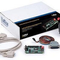
MCU, MPU & DSP Development Tools LatticeXP2 Brevia Dev kit
Manufacturer
Lattice
Series
-r
Type
FPGAr
Datasheets
1.LFXP2-5E-B-EVN.pdf
(25 pages)
2.LFXP2-5E-B-EVN.pdf
(4 pages)
3.LFXP2-5E-B-EVN.pdf
(4 pages)
Specifications of LFXP2-5E-B-EVN
Processor To Be Evaluated
LFXP2-5E-6TN144C
Data Bus Width
8 bit
Interface Type
RS-232, JTAG, SPI
Operating Supply Voltage
3.3 V
Silicon Manufacturer
Lattice Semiconductor
Silicon Family Name
LatticeXP2
Kit Contents
Evaluation Board, USB Cables, AC Adapter, Quick Start Guide
Features
Serial RS232 Interface, JTAG Interface
Svhc
No
Rohs Compliant
Yes
Contents
Board, Cables, Documentation, Power Supply
Lead Free Status / RoHS Status
Lead free / RoHS Compliant
For Use With/related Products
LFXP2-5E-6TN144C
Available stocks
Company
Part Number
Manufacturer
Quantity
Price
Company:

Part Number:
LFXP2-5E-B-EVN
Manufacturer:
Lattice
Quantity:
8


flexiFLASH Architecture
Instant-on (1ms), small-form-factor chip
with support for high-speed 7:1 LVDS
(840 Mbps) interface.
Device Selection Guide
1. Available as automotive temperature range-qualified packages, except for LatticeXP2-30. All packages are available in standard commercial or industrial temperature ranges.
Applications Support
1-800-LATTICE (528-8423)
(503) 268-8001
techsupport@latticesemi.com
www.latticesemi.com
Copyright © 2010 Lattice Semiconductor Corporation. Lattice Semiconductor, L (stylized) Lattice Semiconductor Corp., and Lattice (design), flexiFLASH,
FlashBAK, ispLEVER, ispLeverCORE, LatticeECP2, LatticeMico32, LatticeXP, LatticeXP2, sysCLOCK, sysDSP, sysIO, sysMEM, and TransFR are either
registered trademarks or trademarks of Lattice Semiconductor Corporation in the United States and/or other countries. Other product names used in this
publication are for identification purposes only and may be trademarks of their respective companies. Printed in China.
Advantages of the LatticeXP2 Platform
Fast parallel data
transfer for instant-on.
Device lock for design
security.
LUTs (K)
sysMEM EBR RAM Blocks
Embedded Memory (Kbits)
Distributed Memory (Kbits)
sysDSP Blocks
Number of 18x18 Multipliers
Number of PLLs
Vcc Voltage (V)
Packages & I/O Combinations
132-ball csBGA (8 x 8 mm)
144-pin TQFP (20 x 20 mm)
208-pin PQFP (28 x 28 mm)
256-ball ftBGA (17 x 17 mm)
484-ball fpBGA (23 x 23 mm)
672-ball fpBGA (27 x 27 mm)
Decryption & Device Lock
Configuration Bits
EBR Blocks
EBR Blocks
SRAM
Parameter
FlashBAK for sysMEM
EBR storage.
Flash for single
chip solution.
1
1
1
1
Memory
TAG
SPI &
JTAG
128-Bit AES Bitstream Encryption
Design security ensured by a robust 128-
bit AES bitstream encryption and design-
specific key.
Encrypted Bitsteam
LFXP2-5
128 Bit AES
166
100
146
172
1.2
10
12
86
5
9
3
2
Design specific key stored in
on-chip Flash.
Decryption
Engine
128-Bit
Key
LFXP2-8
e
221
100
146
201
LatticeXP2
1.2
12
18
16
86
8
4
2
(Configuration)
Logic – SRAM
FLASH
LFXP2-17
276
146
201
358
1.2
17
15
35
20
5
4
TransFR Technology
TransFR technology enables the
LatticeXP2 FPGAs to be re-programmed
while your system continues to operate.
While the device is operating,
Load New Configuration (2)
Transfer New Configuration
LatticeXP2 FPGA Regains
to Configuration Memory
the Desired States
Lock the I/Os in
Control of I/Os
to Logic
LFXP2-30
Step 1
Step 2
Step 3
Step 4
387
201
363
472
1.2
29
21
56
28
7
4
(Configuration 2)
(Configuration 1)
(Configuration 2)
(Configuration 2)
LFXP2-40
LatticeXP2
LatticeXP2
Logic – SRAM
Logic – SRAM
FLASH
FLASH
885
363
540
Order #: I0192B
1.2
40
48
83
32
8
4
May 2010
Related parts for LFXP2-5E-B-EVN
Image
Part Number
Description
Manufacturer
Datasheet
Request
R

Part Number:
Description:
FPGA - Field Programmable Gate Array 5K LUTs 146I/O Inst- on DSP 1.2V -5 Spd
Manufacturer:
Lattice
Datasheet:

Part Number:
Description:
Programmable Logic IC Development Tools Lattice XP2 Brevia Dev Kit
Manufacturer:
Lattice
Datasheet:

Part Number:
Description:
FPGA - Field Programmable Gate Array 5K LUTs 172 I/O Inst on DSP 1.2V -5 Spd
Manufacturer:
Lattice
Datasheet:
Part Number:
Description:
FPGA - Field Programmable Gate Array 5K LUTs 100 I/O Inst on DSP 1.2V -5 Spd
Manufacturer:
Lattice
Datasheet:

Part Number:
Description:
FPGA - Field Programmable Gate Array 5K LUTs 172I/O Inst- on DSP 1.2V -5 Spd
Manufacturer:
Lattice
Datasheet:

Part Number:
Description:
FPGA - Field Programmable Gate Array 5K LUTs 100I/O Inst- on DSP 1.2V -5 Spd
Manufacturer:
Lattice
Datasheet:

Part Number:
Description:
FPGA LatticeXP2 Family 5000 Cells Flash Technology 1.2V 256-Pin FTBGA
Manufacturer:
LATTICE SEMICONDUCTOR
Datasheet:
Part Number:
Description:
FPGA LatticeXP2 Family 5000 Cells Flash Technology 1.2V 256-Pin FTBGA
Manufacturer:
LATTICE SEMICONDUCTOR
Datasheet:
Part Number:
Description:
IC DSP 5KLUTS 100I/O 144TQFP
Manufacturer:
Lattice
Datasheet:
Part Number:
Description:
IC DSP 5KLUTS 86I/O 132CSBGA
Manufacturer:
Lattice
Datasheet:
Part Number:
Description:
IC DSP 5KLUTS 86I/O 132CSBGA
Manufacturer:
Lattice
Datasheet:
Part Number:
Description:
IC DSP 5KLUTS 146I/O 208PQFP
Manufacturer:
Lattice
Datasheet:
Part Number:
Description:
IC DSP 5KLUTS 146I/O 208PQFP
Manufacturer:
Lattice
Datasheet:
Part Number:
Description:
IC DSP 5KLUTS 172I/O 256FTBGA
Manufacturer:
Lattice
Datasheet:
Part Number:
Description:
IC FPGA 5KLUTS 86I/O 132-BGA
Manufacturer:
Lattice
Datasheet: