LFXP2-5E-B-EVN Lattice, LFXP2-5E-B-EVN Datasheet - Page 2
LFXP2-5E-B-EVN
Manufacturer Part Number
LFXP2-5E-B-EVN
Description
MCU, MPU & DSP Development Tools LatticeXP2 Brevia Dev kit
Manufacturer
Lattice
Series
-r
Type
FPGAr
Datasheets
1.LFXP2-5E-B-EVN.pdf
(25 pages)
2.LFXP2-5E-B-EVN.pdf
(4 pages)
3.LFXP2-5E-B-EVN.pdf
(4 pages)
Specifications of LFXP2-5E-B-EVN
Processor To Be Evaluated
LFXP2-5E-6TN144C
Data Bus Width
8 bit
Interface Type
RS-232, JTAG, SPI
Operating Supply Voltage
3.3 V
Silicon Manufacturer
Lattice Semiconductor
Silicon Family Name
LatticeXP2
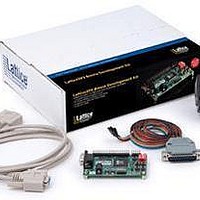
Kit Contents
Evaluation Board, USB Cables, AC Adapter, Quick Start Guide
Features
Serial RS232 Interface, JTAG Interface
Svhc
No
Rohs Compliant
Yes
Contents
Board, Cables, Documentation, Power Supply
Lead Free Status / RoHS Status
Lead free / RoHS Compliant
For Use With/related Products
LFXP2-5E-6TN144C
Available stocks
Company
Part Number
Manufacturer
Quantity
Price
Company:

Part Number:
LFXP2-5E-B-EVN
Manufacturer:
Lattice
Quantity:
8


sysCLOCK PLL BLOCK DIAGRAM
LatticeXP2 Architecture
Architecture Overview
LatticeXP2 FPGAs combine on-chip Flash memory with SRAM programmable LUTs and
interconnect to provide an optimized low cost architecture that delivers high perfor-
mance sysMEM embedded RAM blocks, distributed memory, sysCLOCK PLLs, DDR
memory interface, sysIO buffers, and more.
PFU BLOCK DIAGRAM
Feedback
sysIO BLOCK DIAGRAM
Fabric
FPGA
Control
Signals
Clock
Reset
Input
Routing
Clock
From
Internal Feedback
(Optional)
Gearbox
Carry Chain
2:1
LUT4
LUT4
LUT4
LUT4
LUT4
LUT4
LUT4
LUT4
DQS/Strobe Delay &
Frequency
Detector /
Oscillator
Transition Detect
Voltage
Control
Phase
Carry Chain
Output Register
Register Block
Input Register
(2 Flip/Flops)
(2 Flip/Flops)
(5 Flip/Flops)
Tri-State
Block
Block
Duty Cycle/
Slice 3
Slice 2
Slice 1
Slice 0
Duty Trim
Duty Trim
Phase/
FF
FF
FF
FF
FF
FF
Divider
Lock Detect
Routing
÷3
To
sysMEM
Embedded Block
RAM (EBR)
provides up to
885 Kbits with
speeds up to
350MHz.
Programmable
Function Units
(PFUs) provide up
to 40K LUTs and
speeds up to
350MHz.
LatticeXP2 Block Diagram
sysIO Buffers
support LVCMOS,
HSTL, SSTL,
LVDS, and more.
sysDSP BLOCK DIAGRAM
On-chip
Oscillator
Multipliers
sysDSP Blocks include
multiply and accumulate,
up to 32 18x18 multipliers,
and speeds up to 325MHz.
Pipeline Registers
Accumulator
Subtractor/
Adder/
+ - ∑
+ - ∑
Pre-Engineered Source
Synchronous I/O supports
DDR/DDR2 & 7:1 LVDS.
Summation
+
JTAG and SPI Ports
with Live Update
technology.
Serial TAG Memory
FPGA
Logic
JTAG
JTAG
TA
TA
TDI
Register (Nx8)
Data Shift
Memory
flexiFLASH architecture
offers a secure, instant-on,
single chip solution.
LatticeXP2 FPGAs offer
the best of both worlds,
with the instant-on, non-
volatility of Flash and the
reconfigurability of SRAM
– all in one chip.
Flash
Array
sysCLOCK PLLs for
clock management.
Up to 4 per device.
TDO
JTAG
FPGA
Logic
Related parts for LFXP2-5E-B-EVN
Image
Part Number
Description
Manufacturer
Datasheet
Request
R

Part Number:
Description:
FPGA - Field Programmable Gate Array 5K LUTs 146I/O Inst- on DSP 1.2V -5 Spd
Manufacturer:
Lattice
Datasheet:

Part Number:
Description:
Programmable Logic IC Development Tools Lattice XP2 Brevia Dev Kit
Manufacturer:
Lattice
Datasheet:

Part Number:
Description:
FPGA - Field Programmable Gate Array 5K LUTs 172 I/O Inst on DSP 1.2V -5 Spd
Manufacturer:
Lattice
Datasheet:
Part Number:
Description:
FPGA - Field Programmable Gate Array 5K LUTs 100 I/O Inst on DSP 1.2V -5 Spd
Manufacturer:
Lattice
Datasheet:

Part Number:
Description:
FPGA - Field Programmable Gate Array 5K LUTs 172I/O Inst- on DSP 1.2V -5 Spd
Manufacturer:
Lattice
Datasheet:

Part Number:
Description:
FPGA - Field Programmable Gate Array 5K LUTs 100I/O Inst- on DSP 1.2V -5 Spd
Manufacturer:
Lattice
Datasheet:

Part Number:
Description:
FPGA LatticeXP2 Family 5000 Cells Flash Technology 1.2V 256-Pin FTBGA
Manufacturer:
LATTICE SEMICONDUCTOR
Datasheet:
Part Number:
Description:
FPGA LatticeXP2 Family 5000 Cells Flash Technology 1.2V 256-Pin FTBGA
Manufacturer:
LATTICE SEMICONDUCTOR
Datasheet:
Part Number:
Description:
IC DSP 5KLUTS 100I/O 144TQFP
Manufacturer:
Lattice
Datasheet:
Part Number:
Description:
IC DSP 5KLUTS 86I/O 132CSBGA
Manufacturer:
Lattice
Datasheet:
Part Number:
Description:
IC DSP 5KLUTS 86I/O 132CSBGA
Manufacturer:
Lattice
Datasheet:
Part Number:
Description:
IC DSP 5KLUTS 146I/O 208PQFP
Manufacturer:
Lattice
Datasheet:
Part Number:
Description:
IC DSP 5KLUTS 146I/O 208PQFP
Manufacturer:
Lattice
Datasheet:
Part Number:
Description:
IC DSP 5KLUTS 172I/O 256FTBGA
Manufacturer:
Lattice
Datasheet:
Part Number:
Description:
IC FPGA 5KLUTS 86I/O 132-BGA
Manufacturer:
Lattice
Datasheet: