LFXP2-5E-B-EVN Lattice, LFXP2-5E-B-EVN Datasheet

MCU, MPU & DSP Development Tools LatticeXP2 Brevia Dev kit

LFXP2-5E-B-EVN

Manufacturer Part Number
LFXP2-5E-B-EVN
Description
MCU, MPU & DSP Development Tools LatticeXP2 Brevia Dev kit
Manufacturer
Lattice
Series
-r
Type
FPGAr

Specifications of LFXP2-5E-B-EVN

Processor To Be Evaluated
LFXP2-5E-6TN144C
Data Bus Width
8 bit
Interface Type
RS-232, JTAG, SPI
Operating Supply Voltage
3.3 V
Silicon Manufacturer
Lattice Semiconductor
Silicon Family Name
LatticeXP2
Kit Contents
Evaluation Board, USB Cables, AC Adapter, Quick Start Guide
Features
Serial RS232 Interface, JTAG Interface
Svhc
No
Rohs Compliant
Yes
Contents
Board, Cables, Documentation, Power Supply
Lead Free Status / RoHS Status
Lead free / RoHS Compliant
For Use With/related Products
LFXP2-5E-6TN144C

Available stocks

Company
Part Number
Manufacturer
Quantity
Price
Part Number:
LFXP2-5E-B-EVN
Manufacturer:
Lattice
Quantity:
8
LatticeXP2 Family
Instant-On, Secure, Single-Chip FPGA with Complete Development Platform
L O W - C O S T , 3 R D G E N E R A T I O N , N O N - V O L A T I L E F P G A
LatticeXP2™ is an instant-on, secure, small-form-factor
FPGA with a versatile development platform for quick
launch of design initiatives and rapid time-to-market.
LatticeXP2 offers twice as many logic and signal processing
resources for seamless design upgrades from highly popular
MachXO devices. The high-speed 7:1 LVDS interface enables
rapid image data transfer in video applications. The Lattice-
Mico32™ soft processor allows the LatticeXP2 to be used
even as a microcontroller.
LatticeXP2 devices are based on Lattice’ s unique flexi-
FLASH™ architecture that combines a 4-input Look-up
Table (LUT) based FPGA fabric with non-volatile Flash cells
for on-chip storage of design data. The flexiFLASH architec-
ture provides distributed and embedded memory, enhanced
sysDSP™ blocks, Phase Locked Loops (PLLs), pre-engi-
neered source synchronous I/Os. The versatile I/Os support
DDR/DDR2 & 7:1 LVDS.
In addition, the LatticeXP2 devices have access to gen-
eral-purpose Serial TAG memory, inherent design secu-
rity, 128-bit AES bitstream encryption, Live Update field
reconfiguration with TransFR™, and Dual Boot technologies.
The Lattice ispLEVER
to be efficiently implemented using the LatticeXP2 family of
FPGAs. The ispLEVER tool is complemented by pre-designed
IP (Intellectual Property) modules for the LatticeXP2 family.
By using these standardized IP blocks, designers are free to
concentrate on the unique aspects of their design, increasing
their productivity.
Complete Non-Volatile System-on-Chip
Pre-engineered Source
Synchronous I/O
Live Update via Ethernet
Typical LatticeXP2 Application – Remote Sensor Board
DDR2
LVDS
PHY
ADC
SPI
S
7:1
DC
C
Memory Controller
Ethernet MAC
®
(FIR Filter)
DSP Functions in
sysDSP Blocks
400Mbps
750Mbps
Interface
design tool allows complex designs
DSP
Circuit Board
LatticeCORE IP (µP, DDR2, MAC, FIR)
F
LatticeXP2
(FlashBAK Memory)
Power Up Control
LatticeMico32™
Program Code
Instant-on for Integration
of Critical Control Logic
(30K LUTs)
User Logic
(Soft µP)
Key Features and Benefits
flexiFLASH Architecture
• Instant-on (1ms), single chip integration
• High logic-to-I/O ratio
• Embedded & distributed memory
• Flexible, high performance I/Os
Live Update Technology
• TransFR technology – update logic configuration while
• Dual Boot with external SPI Flash improves reliability
• Secure updates with 128 bit AES bitstream encryption
Optimized FPGA Architecture
• Densities from 5K to 40K 4-input Look-up Tables
• Up to 885 Kbits sysMEM™ block RAM
• Up to 83 Kbits distributed RAM
• Low cost TQFP, PQFP and BGA packaging
High Performance sysDSP Block
• Three to eight blocks with multiply and accumulate
• 12 to 32 18x18 multipliers
Flexible sysIO™ Buffer Supports:
– LVCMOS 3.3/2.5/1.8/1.5/1.2; LVTTL
– SSTL 18 class I, II; SSTL 3/2 class I, II
– HSTL15 class I; HSTL18 class I, II
– PCI
– LVDS, Bus-LVDS, LVPECL
Pre-engineered Source Synchronous Interfaces
• DDR / DDR2 up to 200MHz/400Mbps
• 7:1 LVDS up to 600Mbps
• Generic up to 750Mbps
Up to 4 sysCLOCK™ PLLs
System Level Support
• SPI/JTAG interface for device programming
• IEEE Standard 1149.1 Boundary Scan
• On-board oscillator for initialization & general use
• Soft Error Detect (SED) logic
• 1.2V power supply core voltage
equipment continues to operate
(LUTs)

Related parts for LFXP2-5E-B-EVN

LFXP2-5E-B-EVN Summary of contents

Page 1

... The Lattice- Mico32™ soft processor allows the LatticeXP2 to be used even as a microcontroller. LatticeXP2 devices are based on Lattice’ s unique flexi- FLASH™ architecture that combines a 4-input Look-up Table (LUT) based FPGA fabric with non-volatile Flash cells for on-chip storage of design data ...

Page 2

... LatticeXP2 Architecture Architecture Overview LatticeXP2 FPGAs combine on-chip Flash memory with SRAM programmable LUTs and interconnect to provide an optimized low cost architecture that delivers high perfor- mance sysMEM embedded RAM blocks, distributed memory, sysCLOCK PLLs, DDR memory interface, sysIO buffers, and more. PFU BLOCK DIAGRAM Carry Chain Slice 3 ...

Page 3

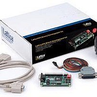
... QuickSTART Guide, and demonstration design JTAG DIP Header Switch Board Shown Actual Size inches 5 x 7.6 cm 2x5 Expansion Status LEDs Header LED Bank Other Functional Block RS-232/USB SRAM Memory JTAG/USB Controller SRAM Switch Memory PC Host Bank (1Mbit) 2x5 Expansion Header Ordering Part # LFXP2-5E-B-EVN ...

Page 4

... Lock the I/Os in the Desired States Step 3 Transfer New Configuration LatticeXP2 to Logic FLASH (Configuration 2) Step 4 Logic – SRAM LatticeXP2 FPGA Regains (Configuration 2) Control of I/Os TransFR technology enables the LatticeXP2 FPGAs to be re-programmed while your system continues to operate. LFXP2-30 LFXP2- 276 387 885 ...

Related keywords