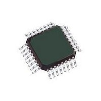
KIT33912G5DGEVME Freescale Semiconductor, KIT33912G5DGEVME Datasheet - Page 14

KIT33912G5DGEVME
Manufacturer Part Number
KIT33912G5DGEVME
Description
Power Management Modules & Development Tools 33912G5 LIN SBC KIT
Manufacturer
Freescale Semiconductor
Type
Motor / Motion Controllers & Driversr
Specifications of KIT33912G5DGEVME
Interface Type
SPI
Product
Power Management Modules
Silicon Manufacturer
Freescale
Silicon Core Number
MC33912
Kit Application Type
Interface
Application Sub Type
LIN System
Kit Contents
Board, CD, Misc Cable
Rohs Compliant
Yes
For Use With/related Products
MC33912
Lead Free Status / RoHS Status
Lead free / RoHS Compliant
Table 4. Static Electrical Characteristics (continued)
34912, unless otherwise noted. Typical values noted reflect the approximate parameter mean at T
conditions, unless otherwise noted.
14
33912
ANALOG OUTPUTS (ADOUT0 AND ADOUT1)
CURRENT SENSE AMPLIFIER (ISENSEH, ISENSEL)
RXD OUTPUT PIN (LIN PHYSICAL LAYER) (RXD)
TXD INPUT PIN (LIN PHYSICAL LAYER) (TXD)
LIN PHYSICAL LAYER WITH J2602 FEATURE ENABLED (BIT DIS_J2602 = 0)
Notes
ELECTRICAL CHARACTERISTICS
STATIC ELECTRICAL CHARACTERISTICS
VSENSE Input Divider Ratio (RATIOVSENSE=V
characterization
VSENSE Output Related Offset
V
Maximum Output Voltage
Minimum Output Voltage
Gain
Differential Input Impedance
Common Mode Input Impedance
ISENSEH, ISENSEL Input Voltage Range
Input Offset Voltage
Low-state Output Voltage
High-state Output Voltage
Low-state Input Voltage
High-state Input Voltage
Pin Pull-up Current, 0 V < V
LIN Under-voltage threshold
Hysteresis (V
40.
Characteristics noted under conditions 5.5 V ≤ V
SENSE
5.5 <V
-5.0 mA < I
-5.0 mA < I
CSGS (Current Sense Gain Select) = 0
CSGS (Current Sense Gain Select) = 1
CSGS (Current Sense Gain Select) = 0
CSGS (Current Sense Gain Select) = 1
CSGS (Current Sense Gain Select) = 0
CSGS (Current Sense Gain Select) = 1
CSAZ (Current Sense Auto Zero) = 0
CSAZ (Current Sense Auto Zero) = 1
I
I
Positive and Negative threshold (V
OUT
OUT
These limits have been defined after laboratory characterization on 3 lots and 30 samples. These tighten limits could not be guaranteed
by production test.
= 1.5 mA
= -250 µA
Output Related Offset per characterization
SUP
< 27 V
THP
O
O
(40)
< 5.0 mA
< 5.0 mA
- V
THN
)
Characteristic
IN
< 3.5 V
THP
, V
THN
)
SENSE
(40)
/V
SUP
ADOUT0
≤ 18 V, -40°C ≤ T
) per
OFFSET
OFFSET
V
RATIO
TH_UNDER_VOL
V
V
V
V
IN_OFFSET
Symbol
J2602_DEG
OUT_MAX
OUT_MIN
DIFF
I
TAGE
V
V
_CZ
CM
PUIN
A
V
V
V
VSENSEC
G
Z
OL
OH
IN
IH
IL
≤ 125°C for the 33912 and -40°C ≤ T
VSENSE
VSENSE
V
0.7 x V
V
DD
DD
5.15
Min
-0.2
-2.0
-0.3
100
100
-30
-30
0.0
2.0
5.0
-15
0.0
5.0
29
14
10
-
-0.35
-0.8
Analog Integrated Circuit Device Data
DD
-12.6
5.25
14.5
Typ
400
-10
30
10
20
20
A
–
–
–
–
–
–
–
–
–
–
–
-
= 25°C under nominal
Freescale Semiconductor
0.3 x V
V
DD
Max
5.35
0.35
V
V
200
200
3.0
2.0
0.8
6.0
30
31
15
30
50
15
30
0
DD
DD
-
+0.3
A
DD
≤ 85°C for the
Unit
mV
mV
mV
mV
kΩ
kΩ
µA
V
V
V
V
V
V
V
V


