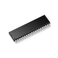
AT89LP52-20PU Atmel, AT89LP52-20PU Datasheet - Page 35

AT89LP52-20PU
Manufacturer Part Number
AT89LP52-20PU
Description
IC MCU 8051 8K FLASH SPI 40PDIP
Manufacturer
Atmel
Series
89LPr
Datasheet
1.AT89LP52-20MU.pdf
(113 pages)
Specifications of AT89LP52-20PU
Core Processor
8051
Core Size
8-Bit
Speed
20MHz
Connectivity
EBI/EMI, I²C, SPI, UART/USART
Peripherals
Brown-out Detect/Reset, POR, PWM, WDT
Number Of I /o
36
Program Memory Size
8KB (8K x 8)
Program Memory Type
FLASH
Ram Size
256 x 8
Voltage - Supply (vcc/vdd)
2.4 V ~ 5.5 V
Oscillator Type
Internal
Operating Temperature
-40°C ~ 85°C
Package / Case
40-DIP (0.600", 15.24mm)
Processor Series
AT89x
Core
8051
Data Bus Width
8 bit
Data Ram Size
256 B
Interface Type
Serial
Maximum Clock Frequency
20 MHz
Number Of Programmable I/os
36
Number Of Timers
3
Operating Supply Voltage
2.7 V to 5.5 V
Maximum Operating Temperature
+ 85 C
Mounting Style
Through Hole
Lead Free Status / RoHS Status
Lead free / RoHS Compliant
Eeprom Size
-
Data Converters
-
Lead Free Status / Rohs Status
Details
8.2.1
8.2.2
3709B–MICRO–12/10
Interrupt Recovery from Power-down
Reset Recovery from Power-down
Two external interrupt sources may be configured to terminate Power-down mode: external
interrupts INT0 (P3.2) and INT1 (P3.3). To wake up by external interrupt INT0 or INT1, that inter-
rupt must be enabled by setting EX0 or EX1 in IE and must be configured for level-sensitive
operation by clearing IT0 or IT1.
When terminating Power-down by an interrupt, two different wake-up modes are available.
When PWDEX in PCON is one, the wake-up period is internally timed as shown in
the falling edge on the interrupt pin, Power-down is exited, the oscillator is restarted, and an
internal timer begins counting. The internal clock will not be allowed to propagate to the CPU
until after the timer has timed out. After the time-out period the interrupt service routine will
begin. The time-out period is controlled by the Start-up Timer Fuses (see
The interrupt pin need not remain low for the entire time-out period.
Figure 8-1.
When PWDEX = “0”, the wake-up period is controlled externally by the interrupt. Again, at the
falling edge on the interrupt pin, power-down is exited and the oscillator is restarted. However,
the internal clock will not propagate until the rising edge of the interrupt pin as shown in
2. The interrupt pin should be held low long enough for the selected clock source to stabilize.
After the rising edge on the pin the interrupt service routine will be executed.
Figure 8-2.
The wake-up from Power-down through an external reset is similar to the interrupt with
PWDEX = “1”. At the rising edge of RST, Power-down is exited, the oscillator is restarted, and
an internal timer begins counting as shown in
propagate to the CPU until after the timer has timed out. The time-out period is controlled by the
Start-up Timer Fuses. (See
clock cycle internal reset is generated when the internal clock restarts. Otherwise, the device will
remain in reset until RST is brought low.
Internal
Internal
XTAL1
XTAL1
Clock
PWD
Clock
INT1
PWD
INT1
Interrupt Recovery from Power-down (PWDEX = 1)
Interrupt Recovery from Power-down (PWDEX = 0)
Table 7-1 on page
AT89LP51/52 - Preliminary
Figure
32). If RST returns low before the time-out, a two
t SUT
8-3. The internal clock will not be allowed to
Table 7-1 on page
Figure
Figure 8-
8-1. At
32).
35


