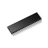
AT89LP52-20PU Atmel, AT89LP52-20PU Datasheet - Page 11

AT89LP52-20PU
Manufacturer Part Number
AT89LP52-20PU
Description
IC MCU 8051 8K FLASH SPI 40PDIP
Manufacturer
Atmel
Series
89LPr
Datasheet
1.AT89LP52-20MU.pdf
(113 pages)
Specifications of AT89LP52-20PU
Core Processor
8051
Core Size
8-Bit
Speed
20MHz
Connectivity
EBI/EMI, I²C, SPI, UART/USART
Peripherals
Brown-out Detect/Reset, POR, PWM, WDT
Number Of I /o
36
Program Memory Size
8KB (8K x 8)
Program Memory Type
FLASH
Ram Size
256 x 8
Voltage - Supply (vcc/vdd)
2.4 V ~ 5.5 V
Oscillator Type
Internal
Operating Temperature
-40°C ~ 85°C
Package / Case
40-DIP (0.600", 15.24mm)
Processor Series
AT89x
Core
8051
Data Bus Width
8 bit
Data Ram Size
256 B
Interface Type
Serial
Maximum Clock Frequency
20 MHz
Number Of Programmable I/os
36
Number Of Timers
3
Operating Supply Voltage
2.7 V to 5.5 V
Maximum Operating Temperature
+ 85 C
Mounting Style
Through Hole
Lead Free Status / RoHS Status
Lead free / RoHS Compliant
Eeprom Size
-
Data Converters
-
Lead Free Status / Rohs Status
Details
3.1.1
3709B–MICRO–12/10
External Program Memory Interface
The AT89LP51/52 uses the standard 8051 external program memory interface with the upper
address on Port 2, the lower address and data in/out multiplexed on Port 0, and the ALE and
PSEN strobes. Program memory addresses are always 16-bits wide, even though the actual
amount of program memory used may be less than 64K byes. External program execution sacri-
fices two full 8-bit ports, P0 and P2, to the function of addressing the program memory.
Figure 3-2
a 16-bit linear address. Port 0 serves as a multiplexed address/data bus to the ROM. The
Address Latch Enable strobe (ALE) is used to latch the lower address byte into an external reg-
ister so that Port 0 can be freed for data input/output. Port 2 provides the upper address byte
throughout the operation. PSEN strobes the external memory.
Figure 3-3
stant rate of 1/3 of the system clock with a 1/3 duty cycle. PSEN is emitted at a similar rate, but
with 50% duty cycle. The new address changes in the middle of the ALE pulse for latching on
the falling edge and is tristated at the falling edge of PSEN. The instruction data is sampled from
P0 and latched internally during the high phase of the clock prior to the rising edge of PSEN.
This timing applies to both Compatibility and Fast modes. In Compatibility mode there is no dif-
ference in instruction timing between internal and external execution.
Figure 3-2.
Figure 3-3.
PSEN
CLK
ALE
shows a hardware configuration for accessing up to 64K bytes of external ROM using
shows the timing of the external program memory interface. ALE is emitted at a con-
P0
P2
Executing from External Program Memory
External Program Memory Fetches
DATA
SAMPLED
PCL
OUT
P1
P3
AT89LP
PSEN
PCH OUT
FLOAT
ALE
P0
P2
AT89LP51/52 - Preliminary
LATCH
DATA
SAMPLED
OUT
PCL
PCH OUT
EXTERNAL
INSTR.
OE
PROGRAM
MEMORY
ADDR
DATA
SAMPLED
OUT
PCL
PCH OUT
11


