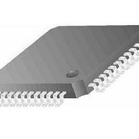
AT89LP52-20AU Atmel, AT89LP52-20AU Datasheet - Page 87

AT89LP52-20AU
Manufacturer Part Number
AT89LP52-20AU
Description
IC MCU 8051 8K FLASH SPI 44TQFP
Manufacturer
Atmel
Series
89LPr
Datasheet
1.AT89LP52-20MU.pdf
(113 pages)
Specifications of AT89LP52-20AU
Core Processor
8051
Core Size
8-Bit
Speed
20MHz
Connectivity
EBI/EMI, I²C, SPI, UART/USART
Peripherals
Brown-out Detect/Reset, POR, PWM, WDT
Number Of I /o
36
Program Memory Size
8KB (8K x 8)
Program Memory Type
FLASH
Ram Size
256 x 8
Voltage - Supply (vcc/vdd)
2.4 V ~ 5.5 V
Oscillator Type
Internal
Operating Temperature
-40°C ~ 85°C
Package / Case
44-TQFP
Processor Series
AT89x
Core
8051
Data Bus Width
8 bit
Data Ram Size
256 B
Interface Type
Serial
Maximum Clock Frequency
20 MHz
Number Of Programmable I/os
36
Number Of Timers
3
Operating Supply Voltage
2.7 V to 5.5 V
Maximum Operating Temperature
+ 85 C
Mounting Style
SMD/SMT
Lead Free Status / RoHS Status
Lead free / RoHS Compliant
Eeprom Size
-
Data Converters
-
Lead Free Status / Rohs Status
Details
Available stocks
Company
Part Number
Manufacturer
Quantity
Price
Company:
Part Number:
AT89LP52-20AU
Manufacturer:
Atmel
Quantity:
250
Table 17-5.
Notes:
17.8
17.9
17.9.1
3709B–MICRO–12/10
Address
07H
08H
09H
1. The default state for all fuses is FFh.
2. Changes to these fuses will only take effect after a device POR.
3. Changes to these fuses will only take effect after the ISP session terminates by bringing RST inactive.
User Signature
Programming Interface Timing
Power-up Sequence
Fuse Name
Tristate Ports
In-Application Programming
R1 Enable
User Configuration Fuse Definitions
The User Signature Array contains 256 bytes of non-volatile memory in two 128-byte pages. The
User Signature is available for serial numbers, firmware revision information, date codes or other
user parameters. The User Signature Array may only be written by an external device when the
User Signature Programming Fuse is enabled. When the fuse is enabled, Chip Erase will also
erase the first page of the array. When the fuse is disabled, the array is not affected by write or
erase commands. Programming of the Signature Array can also be disabled by the Lock Bits.
However, reading the signature is always allowed and the array should not be used to store
security sensitive information. The User Signature Array may be modified during execution
through the In-Application Programming interface, regardless of the state of the User Signature
Programming fuse or Lock Bits, provided that the IAP Fuse is enabled. Note that the address of
the User Signature Array, as seen by the IAP interface, equals the User Signature address plus
256 (0100H–01FFH instead of 0000H–00FFH).
This section details general system timing sequences and constraints for entering or exiting In-
System Programming as well as parameters related to the Serial Peripheral Interface during
ISP. The general timing parameters for the following waveform figures are listed in section
ing Parameters” on page
Execute this sequence to enter programming mode immediately after power-up. In the RST pin
is disabled or if the ISP Fuse is disabled, this is the only method to enter programming (see
“External Reset” on page
1. Apply power between VDD and GND pins. RST should remain low.
2. Wait at least t
3. Wait at least t
4. Start programming session.
depend on the current settings of the device.
PWRUP
SUT
Description
FFh: I/O Ports start in input-only mode (tristated) after reset
00h: I/O Ports start in quasi-bidirectional mode after reset
FFh: In-Application Programming Disabled
00h: In-Application Programming Enabled
FFh: 5 MΩ resistor on XTAL1 Disabled
00h: 5 MΩ resistor on XTAL1 Enabled
for the internal Power-on Reset to complete. The value of t
. and drive RST high if active-high otherwise keep low.
91.
32).
AT89LP51/52 - Preliminary
SUT
will
“Tim-
87


