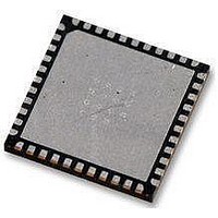
AT89LP52-20MU Atmel, AT89LP52-20MU Datasheet - Page 17

AT89LP52-20MU
Manufacturer Part Number
AT89LP52-20MU
Description
IC MCU 8051 8K FLASH SPI 44VQFN
Manufacturer
Atmel
Series
89LPr
Datasheet
1.AT89LP52-20MU.pdf
(113 pages)
Specifications of AT89LP52-20MU
Core Processor
8051
Core Size
8-Bit
Speed
20MHz
Connectivity
EBI/EMI, I²C, SPI, UART/USART
Peripherals
Brown-out Detect/Reset, POR, PWM, WDT
Number Of I /o
36
Program Memory Size
8KB (8K x 8)
Program Memory Type
FLASH
Ram Size
256 x 8
Voltage - Supply (vcc/vdd)
2.4 V ~ 5.5 V
Oscillator Type
Internal
Operating Temperature
-40°C ~ 85°C
Package / Case
44-VFQFN Exposed Pad
Processor Series
AT89x
Core
8051
Data Bus Width
8 bit
Data Ram Size
256 B
Interface Type
Serial
Maximum Clock Frequency
20 MHz
Number Of Programmable I/os
36
Number Of Timers
3
Operating Supply Voltage
2.7 V to 5.5 V
Maximum Operating Temperature
+ 85 C
Mounting Style
SMD/SMT
Lead Free Status / RoHS Status
Lead free / RoHS Compliant
Eeprom Size
-
Data Converters
-
Lead Free Status / Rohs Status
Details
Available stocks
Company
Part Number
Manufacturer
Quantity
Price
Company:
Part Number:
AT89LP52-20MU
Manufacturer:
Atmel
Quantity:
490
Table 3-2.
3.3.3
3709B–MICRO–12/10
Symbol
IAP
AERS
LDPG
MWEN
DMEN
ERR
BUSY
WRTINH
MEMCON = 96H
Not Bit Addressable
Bit
External Data Memory Interface
Function
In-Application Programming Enable. When IAP = 1 and the IAP Fuse is enabled, programming of the CODE/SIG space
is enabled and MOVX @DPTR instructions will access CODE/SIG instead of EDATA or FDATA. Clear IAP to disable
programming of CODE/SIG and allow access to EDATA and FDATA.
Auto-Erase Enable. Set to perform an auto-erase of a Flash memory page (CODE, SIG or FDATA) during the next write
sequence. Clear to perform write without erase.
Load Page Enable. Set to this bit to load multiple bytes to the temporary page buffer. Byte locations may not be loaded
more than once before a write. LDPG must be cleared before writing.
Memory Write Enable. Set to enable programming of a nonvolatile memory location (CODE, SIG or FDATA). Clear to
disable programming of all nonvolatile memories.
Data Memory Enable. Set to enable nonvolatile data memory and map it into the FDATA space. Clear to disable
nonvolatile data memory.
Error Flag. Set by hardware if an error occurred during the last programming sequence due to a brownout condition (low
voltage on VDD). Must be cleared by software.
Busy Flag.
Write Inhibit Flag. Cleared by hardware when the voltage on VDD has fallen below the minimum programming voltage.
Set by hardware when the voltage on VDD is above the minimum programming voltage.
MEMCON
IAP
7
– Memory Control Register
The AT89LP51/52 uses the standard 8051 external data memory interface with the upper
address on Port 2, the lower address and data in/out multiplexed on Port 0, and the ALE, RD
and WR strobes. The interface may be used in two different configurations depending on which
type of MOVX instruction is used to access XDATA.
Figure 3-10
using a 16-bit linear address. Port 0 serves as a multiplexed address/data bus to the RAM. The
Address Latch Enable strobe (ALE) is used to latch the lower address byte into an external reg-
ister so that Port 0 can be freed for data input/output. Port 2 provides the upper address byte
throughout the operation. The MOVX @DPTR instructions use Linear Address mode.
AERS
6
shows a hardware configuration for accessing up to 64K bytes of external RAM
LDPG
5
MWEN
4
DMEN
3
AT89LP51/52 - Preliminary
ERR
2
Reset Value = 0000 0XXXB
BUSY
1
WRTINH
0
17


