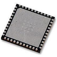
AT89LP52-20MU Atmel, AT89LP52-20MU Datasheet - Page 15

AT89LP52-20MU
Manufacturer Part Number
AT89LP52-20MU
Description
IC MCU 8051 8K FLASH SPI 44VQFN
Manufacturer
Atmel
Series
89LPr
Datasheet
1.AT89LP52-20MU.pdf
(113 pages)
Specifications of AT89LP52-20MU
Core Processor
8051
Core Size
8-Bit
Speed
20MHz
Connectivity
EBI/EMI, I²C, SPI, UART/USART
Peripherals
Brown-out Detect/Reset, POR, PWM, WDT
Number Of I /o
36
Program Memory Size
8KB (8K x 8)
Program Memory Type
FLASH
Ram Size
256 x 8
Voltage - Supply (vcc/vdd)
2.4 V ~ 5.5 V
Oscillator Type
Internal
Operating Temperature
-40°C ~ 85°C
Package / Case
44-VFQFN Exposed Pad
Processor Series
AT89x
Core
8051
Data Bus Width
8 bit
Data Ram Size
256 B
Interface Type
Serial
Maximum Clock Frequency
20 MHz
Number Of Programmable I/os
36
Number Of Timers
3
Operating Supply Voltage
2.7 V to 5.5 V
Maximum Operating Temperature
+ 85 C
Mounting Style
SMD/SMT
Lead Free Status / RoHS Status
Lead free / RoHS Compliant
Eeprom Size
-
Data Converters
-
Lead Free Status / Rohs Status
Details
Available stocks
Company
Part Number
Manufacturer
Quantity
Price
Company:
Part Number:
AT89LP52-20MU
Manufacturer:
Atmel
Quantity:
490
AT89LP51/52 - Preliminary
peripherals will continue to function during the write cycle; however, interrupts will not be ser-
viced until the write completes.
For external execution the AT89LP51/52 uses an execute-while-write architecture where the
CPU continues to operate while the write occurs. The software should poll the state of the BUSY
flag to determine when the write completes. Interrupts must be disabled during the write
sequence as the CPU will not be able to vector to the internal interrupt table and care should be
taken that the application does not jump to an internal address until the write completes.
To enable write access to the nonvolatile data memory, the MWEN bit (MEMCON.4) must be set
to one. When MWEN = 1 and DMEN = 1, MOVX @DPTR,A may be used to write to FDATA.
FDATA uses flash memory with a page-based programming model. Flash data memory differs
from traditional EEPROM data memory in the method of writing data. EEPROM generally can
update a single byte with any value. Flash memory splits programming into write and erase
→
operations. A Flash write can only program zeroes, i.e change ones into zeroes (
). Any
1
0
ones in the write data are ignored. A Flash erase sets an entire page of data to ones so that all
bytes become FFH. Therefore after an erase, each byte in the page can only be written once
with any possible value. Bytes can be overwritten without an erase as long as only ones are
→
changed into zeroes. However, if even a single bit needs updating from zero to one (
);
0
1
then the contents of the page must first be saved, the entire page must be erased and the zero
bits in all bytes (old and new data combined) must be written. Avoiding unnecessary page
erases greatly improves the endurance of the memory..
The AT89LP51/52 includes 2 data pages of 128 bytes each. One or more bytes in a page may
be written at one time. The AT89LP51/52 includes a temporary page buffer of 64 bytes, or half of
a page. Because the page buffer is 64 bytes long, the maximum number of bytes written at one
time is 64. Therefore, two write cycles are required to fill the entire 128-byte page, one for the
low half page (00H–3FH) and one for the high half page (40H–7FH) as shown in
Figure
3-7.
Figure 3-7.
Page Programming Structure
00
3F
Page Buffer
Data Memory
Low Half Page
High Half Page
00
3F
40
7F
The LDPG bit (MEMCON.5) allows multiple data bytes to be loaded to the temporary page buf-
fer. While LDPG = 1, MOVX @DPTR,A instructions will load data to the page buffer, but will not
start a write sequence. Note that a previously loaded byte must not be reloaded prior to the write
sequence. To write the half page into the memory, LDPG must first be cleared and then a
MOVX @DPTR,A with the final data byte is issued. The address of the final MOVX determines
which half page will be written. If a MOVX @DPTR,A instruction is issued while LDPG = 0 with-
out loading any previous bytes, only a single byte will be written. The page buffer is reset after
each write operation.
Figures 3-8 and Figure 3-9 on page 16
show the difference between byte
writes and page writes.
15
3709B–MICRO–12/10


