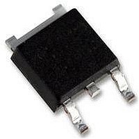
IRLR6225PBF International Rectifier, IRLR6225PBF Datasheet - Page 5

IRLR6225PBF
Manufacturer Part Number
IRLR6225PBF
Description
MOSFET N-CH 20V 100A DPAK
Manufacturer
International Rectifier
Series
HEXFET®r
Datasheet
1.IRLR6225PBF.pdf
(8 pages)
Specifications of IRLR6225PBF
Fet Type
MOSFET N-Channel, Metal Oxide
Fet Feature
Logic Level Gate
Rds On (max) @ Id, Vgs
4 mOhm @ 21A, 4.5V
Drain To Source Voltage (vdss)
20V
Current - Continuous Drain (id) @ 25° C
100A
Vgs(th) (max) @ Id
1.1V @ 50µA
Gate Charge (qg) @ Vgs
72nC @ 4.5V
Input Capacitance (ciss) @ Vds
3770pF @ 10V
Power - Max
63W
Mounting Type
Surface Mount
Package / Case
*
Transistor Polarity
N Channel
Drain Source Voltage Vds
20V
On Resistance Rds(on)
3200µohm
Rds(on) Test Voltage Vgs
4.5V
Operating Temperature Range
-55°C To +150°C
Transistor Case Style
D-PAK
Rohs Compliant
Yes
Resistance Drain-source Rds (on)
4 mOhms
Drain-source Breakdown Voltage
20 V
Gate-source Breakdown Voltage
12 V
Continuous Drain Current
100 A
Power Dissipation
63 W
Mounting Style
SMD/SMT
Gate Charge Qg
48 nC
Lead Free Status / RoHS Status
Lead free / RoHS Compliant
www.irf.com
Fig 14a. Unclamped Inductive Test Circuit
Fig 12. On-Resistance vs. Gate Voltage
Fig 15a. Switching Time Test Circuit
8
7
6
5
4
3
2
1
0
R G
20V
V DS
V GS, Gate -to -Source Voltage (V)
2
t p
≤ 0.1
≤ 1
I AS
D.U.T
4
0.01 Ω
L
6
T J = 125°C
T J = 25°C
8
15V
DRIVER
10
I D = 17A
+
-
+
-
V DD
12
A
14
Fig 13. Maximum Avalanche Energy vs. Drain Current
Fig 14b. Unclamped Inductive Waveforms
700
600
500
400
300
200
100
90%
V
10%
V
I
DS
0
AS
GS
25
Fig 15b. Switching Time Waveforms
Starting T J , Junction Temperature (°C)
t
d(on)
50
t
t p
r
IRLR6225PbF
75
t
100
d(off)
V
(BR)DSS
TOP
BOTTOM 17A
t
f
125
I D
5.9A
8.6A
150
5


