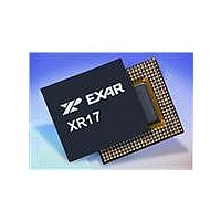
XR17V352IB113-F Exar Corporation, XR17V352IB113-F Datasheet - Page 15

XR17V352IB113-F
Manufacturer Part Number
XR17V352IB113-F
Description
IC UART PCIE 256B DUAL 113FPBGA
Manufacturer
Exar Corporation
Datasheet
1.XR17V352IB113-F.pdf
(64 pages)
Specifications of XR17V352IB113-F
Number Of Channels
2, DUART
Package / Case
113-LFBGA
Features
*
Fifo's
256 Byte
Protocol
RS485
Voltage - Supply
3.3V
With Auto Flow Control
Yes
With Irda Encoder/decoder
Yes
With False Start Bit Detection
Yes
With Modem Control
Yes
Mounting Type
Surface Mount
Data Rate
25 Mbps
Supply Current
120 mA
Maximum Operating Temperature
+ 85 C
Minimum Operating Temperature
- 40 C
Mounting Style
SMD/SMT
Operating Supply Voltage
3.3 V
No. Of Channels
2
Uart Features
Tx/Rx FIFO Counters
Supply Voltage Range
3V To 3.6V
Operating Temperature Range
-40°C To +85°C
Digital Ic Case Style
BGA
No. Of Pins
113
Rohs Compliant
Yes
Lead Free Status / RoHS Status
Lead free / RoHS Compliant
Lead Free Status / RoHS Status
Lead free / RoHS Compliant, Lead free / RoHS Compliant
Available stocks
Company
Part Number
Manufacturer
Quantity
Price
Company:
Part Number:
XR17V352IB113-F
Manufacturer:
EXAR
Quantity:
3 500
Company:
Part Number:
XR17V352IB113-F
Manufacturer:
Exar Corporation
Quantity:
10 000
Part Number:
XR17V352IB113-F
Manufacturer:
EXAR/艾科嘉
Quantity:
20 000
REV. 1.0.1
The Device Configuration Registers provide easy programming of general operating parameters to the V352
and for monitoring the status of various functions. These registers control or report on both channel UARTs
functions that include interrupt control and status, 16-bit general purpose timer control and status, multipurpose
inputs/outputs control and status, sleep mode control, soft-reset control, and device identification and revision,
and others. Tables
registers is described in detail in the following paragraphs.
1.4
A
DDRESS
Ox08C
Ox08D
Ox080
Ox081
Ox082
Ox083
Ox084
Ox085
Ox086
Ox087
Ox088
Ox089
Ox08A
Ox08B
Ox08E
Ox08F
Ox090
Ox091
Ox092
Ox093
Ox095
Ox096
Ox097
0x094
Device Configuration Registers
[A7:A0]
T
ABLE
5
MPIOLVL[15:8]
MPIOINT[15:8]
MPIOSEL[7:0]
and
MPIOLVL[7:0]
MPIOINV[7:0]
MPIO3T[15:8]
MPIOINT[7:0]
MPIOOD[7:0]
TIMERCNTL
MPIO3T[7:0]
INT2 [23:16]
INT3 [31:24]
TIMERMSB
INT1 [15:8]
TIMERLSB
INT0 [7:0]
R
8XMODE
4XMODE
5: D
RESET
SLEEP
EGISTER
REGA
DREV
REGB
DVID
6
EVICE
below show these registers in BYTE and DWORD alignment. Each of these
C
ONFIGURATION
Read-only Interrupt [7:0]
Read-only
Read-only
Read-only
Read/Write Timer Control
Reserved
Read/Write Timer LSB
Read/Write Timer MSB
Individual UART channels can only control the bit
pertaining to that channel in the registers at address
offset 0x088-0x08B.
Read/Write
Read/Write
Write-only Self clear bits after executing Reset
Read/Write Sleep mode
Read-only Device revision
Read-only Device identification
Read/Write EEPROM control
Read/Write MPIO[7:0] interrupt mask
Read/Write MPIO[7:0] level control
Read/Write MPIO[7:0] output control
Read/Write MPIO[7:0] input polarity select
Read/Write MPIO[7:0] select
Read/Write MPIO[7:0] open-drain output control
Read/Write MPIO[15:8] interrupt mask
Read/Write MPIO[15:8] level control
Read/Write MPIO[15:8] output control
R
R
EAD
15
EGISTERS SHOWN IN
HIGH PERFORMANCE DUAL PCI EXPRESS UART
/W
RITE
C
OMMENT
BYTE
ALIGNMENT
Bits [7:0] = Current Rev.
Bits [15:8] = 0x00
Bits [15:8] = 0x00
Bits [15:8] = 0x00
Bits [7:0] = 0xFF
Bits [7:0] = 0x00
Bits [7:0] = 0x00
Bits [7:0] = 0x00
Bits [7:0] = 0x00
Bits [7:0] = 0x00
Bits [7:0] = 0x00
Bits [7:0] = 0x00
Bits [7:0] = 0x00
Bits [7:0] = 0x00
Bits [7:0] = 0x82
Bits [7:0] = 0x00
Bits [7:0] = 0x00
Bits [7:0] = 0x00
Bits [7:0] = 0x00
Bits [7:0] = 0x00
Bits [7:0] = 0x00
Bits [7:0]= 0x00
Bits [7:0]= 0x00
Bits [7:0]= 0x00
RESET STATE
XR17V352


