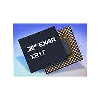
XR17V352IB113-F Exar Corporation, XR17V352IB113-F Datasheet - Page 13

XR17V352IB113-F
Manufacturer Part Number
XR17V352IB113-F
Description
IC UART PCIE 256B DUAL 113FPBGA
Manufacturer
Exar Corporation
Datasheet
1.XR17V352IB113-F.pdf
(64 pages)
Specifications of XR17V352IB113-F
Number Of Channels
2, DUART
Package / Case
113-LFBGA
Features
*
Fifo's
256 Byte
Protocol
RS485
Voltage - Supply
3.3V
With Auto Flow Control
Yes
With Irda Encoder/decoder
Yes
With False Start Bit Detection
Yes
With Modem Control
Yes
Mounting Type
Surface Mount
Data Rate
25 Mbps
Supply Current
120 mA
Maximum Operating Temperature
+ 85 C
Minimum Operating Temperature
- 40 C
Mounting Style
SMD/SMT
Operating Supply Voltage
3.3 V
No. Of Channels
2
Uart Features
Tx/Rx FIFO Counters
Supply Voltage Range
3V To 3.6V
Operating Temperature Range
-40°C To +85°C
Digital Ic Case Style
BGA
No. Of Pins
113
Rohs Compliant
Yes
Lead Free Status / RoHS Status
Lead free / RoHS Compliant
Lead Free Status / RoHS Status
Lead free / RoHS Compliant, Lead free / RoHS Compliant
Available stocks
Company
Part Number
Manufacturer
Quantity
Price
Company:
Part Number:
XR17V352IB113-F
Manufacturer:
EXAR
Quantity:
3 500
Company:
Part Number:
XR17V352IB113-F
Manufacturer:
Exar Corporation
Quantity:
10 000
Part Number:
XR17V352IB113-F
Manufacturer:
EXAR/艾科嘉
Quantity:
20 000
XR17V352
HIGH PERFORMANCE DUAL PCI EXPRESS UART
REV. 1.0.1
1.3
Device Internal Register Sets
The Device Configuration Registers and the two individual UART Configuration Registers of the V352
occupy 2K of PCI bus memory address space. These addresses are offset onto the basic memory address, a
value loaded into the Memory Base Address Register (BAR) in the PCI local bus configuration register set. The
UART Configuration Registers are mapped into 2 address blocks where each UART channel occupies 1024
bytes memory space for its own registers that include the 16550 compatible registers. The Device
Configuration Registers are accessible from both UART channels. However, not all bits can be controlled by
both channels. The UART channel can only control the 8XMODE, 4XMODE, RESET and SLEEP register bits
that apply to that particular channel. For example, this prevents channel 0 from accidentally resetting channel
1.
All these registers can be accessed in 8, 16, 24 or 32 bits width depending on the starting address given by the
host at the beginning of the bus cycle. Transmit and receive data may be loaded or unloaded in 8, 16, 24 or 32
bits format in special locations given in the
Table 4
below. Every time a read or write operation is made to the
transmit or receive register, its FIFO data pointer is automatically bumped to the next sequential data location
either in byte, word or DWORD. One special case applies to the receive data unloading when reading the
receive data together with its LSR register content. The host must read them in 16 or 32 bits format in order to
maintain integrity of the data byte with its associated error flags. These special registers are further discussed
in
“Section 2.1, FIFO DATA LOADING AND UNLOADING IN 32-BIT FORMAT” on page
28.
13


