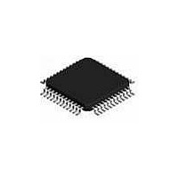
ST16C450CQ48-F Exar Corporation, ST16C450CQ48-F Datasheet - Page 5

ST16C450CQ48-F
Manufacturer Part Number
ST16C450CQ48-F
Description
IC UART SINGLE 48TQFP
Manufacturer
Exar Corporation
Type
UARTsr
Datasheet
1.ST16C450CJ44TR-F.pdf
(28 pages)
Specifications of ST16C450CQ48-F
Package / Case
48-TQFP
Features
*
Number Of Channels
1, UART
Fifo's
1 Byte
Voltage - Supply
2.97 V ~ 5.5 V
With False Start Bit Detection
Yes
With Modem Control
Yes
With Cmos
Yes
Mounting Type
Surface Mount
Data Rate
1.5 Mbps
Supply Current
3 mA
Maximum Operating Temperature
0 C
Minimum Operating Temperature
+ 70 C
Mounting Style
SMD/SMT
Operating Supply Voltage
7 V
Lead Free Status / RoHS Status
Lead free / RoHS Compliant
Lead Free Status / RoHS Status
Lead free / RoHS Compliant, Lead free / RoHS Compliant
Available stocks
Company
Part Number
Manufacturer
Quantity
Price
Company:
Part Number:
ST16C450CQ48-F
Manufacturer:
EXAR
Quantity:
1 400
Company:
Part Number:
ST16C450CQ48-F
Manufacturer:
Exar Corporation
Quantity:
10 000
SYMBOL DESCRIPTION
-IOR
-IOW
INT
CSOUT
-BAUDOUT
-DDIS
-OP1
RESET
RCLK
Symbol
Rev. 4.20
40
21
18
30
24
15
23
34
35
9
Pin
44
20
33
27
17
26
38
39
10
24
23
12
35
48
19
16
30
22
34
5
Signal
type
O
O
O
O
O
I
I
I
I
Read data strobe (active low strobe). A logic 0 on this pin
transfers the contents of the ST16C450 data bus to the
CPU.
Write data strobe (active low strobe). A logic 0 on this pin
transfers the contents of the CPU data bus to the addressed
internal register.
Interrupt Request (active high). Interrupts are enabled in the
interrupt enable register (IER), and when an interrupt con-
dition exists. Interrupt conditions include: receiver errors,
available receiver buffer data, transmit buffer empty, or
when a modem status flag is detected.
Chip select out. A high on this pin indicates that the
ST16C450 has been enabled by the chip select pin.
Baud Rate Generator Output. This pin provides the 16X
clock of the selected data rate from the baud rate generator.
The RCLK pin must be connected externally to -BAUDOUT
when the receiver is operating at the same data rate.
Drive Disable. This pin goes to a logic 0 when the external
CPU is reading data from the ST16C450. This signal can be
used to disable external transceivers or other logic func-
tions.
Output-1 (User Defined) - See bit-2 of modem control
register (MCR bit-2).
Reset. (active high) - A logic 1 on this pin will reset the
internal registers and all the outputs. The UART transmitter
output and the receiver input will be disabled during reset
time. (See ST16C450 External Reset Conditions for initial-
ization details.)
Receive Clock Input. This pin is used as external 16X clock
input to the receiver section. External connection to -
Baudout pin is required in order to utilize the internal baud
rate generator.
5
Pin Description
ST16C450


