ST16C450CQ48-F Exar Corporation, ST16C450CQ48-F Datasheet - Page 13
ST16C450CQ48-F
Manufacturer Part Number
ST16C450CQ48-F
Description
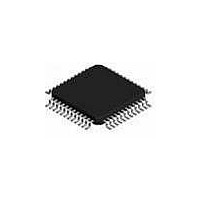
IC UART SINGLE 48TQFP
Manufacturer
Exar Corporation
Type
UARTsr
Datasheet
1.ST16C450CJ44TR-F.pdf
(28 pages)
Specifications of ST16C450CQ48-F
Package / Case
48-TQFP
Features
*
Number Of Channels
1, UART
Fifo's
1 Byte
Voltage - Supply
2.97 V ~ 5.5 V
With False Start Bit Detection
Yes
With Modem Control
Yes
With Cmos
Yes
Mounting Type
Surface Mount
Data Rate
1.5 Mbps
Supply Current
3 mA
Maximum Operating Temperature
0 C
Minimum Operating Temperature
+ 70 C
Mounting Style
SMD/SMT
Operating Supply Voltage
7 V
Lead Free Status / RoHS Status
Lead free / RoHS Compliant
Lead Free Status / RoHS Status
Lead free / RoHS Compliant, Lead free / RoHS Compliant
Available stocks
Company
Part Number
Manufacturer
Quantity
Price
Company:

Part Number:
ST16C450CQ48-F
Manufacturer:
EXAR
Quantity:
1 400
Company:
Part Number:
ST16C450CQ48-F
Manufacturer:
Exar Corporation
Quantity:
10 000


Transmit and Receive Holding Register
The serial transmitter section consists of an 8-bit
Transmit Hold Register (THR) and Transmit Shift
Register (TSR). The status of the THR is provided in
the Line Status Register (LSR). Writing to the THR
transfers the contents of the data bus (D7-D0) to the
THR, providing that the THR or TSR is empty. The
THR empty flag in the LSR register will be set to a logic
1 when the transmitter is empty or when data is
transferred to the TSR. Note that a write operation can
be performed when the transmit holding register
empty flag is set.
The serial receive section also contains an 8-bit
Receive Holding Register, RHR. Receive data is
removed from the ST16C450 and receive by reading
the RHR register. The receive section provides a
mechanism to prevent false starts. On the falling edge
of a start or false start bit, an internal receiver counter
starts counting clocks at 16x clock rate. After 7 1/2
clocks the start bit time should be shifted to the center
of the start bit. At this time the start bit is sampled and
if it is still a logic 0 it is validated. Evaluating the start
bit in this manner prevents the receiver from assem-
bling a false character. Receiver status codes will be
posted in the LSR.
Interrupt Enable Register (IER)
The Interrupt Enable Register (IER) masks the inter-
rupts from receiver ready, transmitter empty, line
status and modem status registers. These interrupts
would normally be seen on the ST16C450 INT output
pin.
IER BIT-0:
Logic 0 = Disable the receiver ready interrupt. (normal
default condition)
Logic 1 = Enable the receiver ready interrupt.
IER BIT-1:
Logic 0 = Disable the transmitter empty interrupt.
(normal default condition)
Logic 1 = Enable the transmitter empty interrupt.
Rev. 4.20
13
IER BIT-2:
Logic 0 = Disable the receiver line status interrupt.
(normal default condition)
Logic 1 = Enable the receiver line status interrupt.
IER BIT-3:
Logic 0 = Disable the modem status register interrupt.
(normal default condition)
Logic 1 = Enable the modem status register interrupt.
IER BIT 4-7: Not used and set to “0”.
Interrupt Status Register (ISR)
The ST16C450 provides four levels of prioritized
interrupts to minimize external software interaction.
The Interrupt Status Register (ISR) provides the user
with four interrupt status bits. Performing a read cycle
on the ISR will provide the user with the highest
pending interrupt level to be serviced. No other inter-
rupts are acknowledged until the pending interrupt is
serviced. Whenever the interrupt status register is
read, the interrupt status is cleared. However it should
be noted that only the current pending interrupt is
cleared by the read. A lower level interrupt may be seen
after rereading the interrupt status bits. The Interrupt
Source Table 5 (below) shows the data values (bit 0-3)
for the four prioritized interrupt levels and the interrupt
sources associated with each of these interrupt levels:
ST16C450
Related parts for ST16C450CQ48-F
Image
Part Number
Description
Manufacturer
Datasheet
Request
R

Part Number:
Description:
UNIVERSAL ASYNCHRONOUS RECEIVER/TRANSMITTER (UART)
Manufacturer:
Exar Corporation
Datasheet:
Part Number:
Description:
BiCMOS Fixed, Quad, Voltage Output, Single or Dual Supply 8-Bit Digital-to-Analog Converter
Manufacturer:
Exar Corporation
Datasheet:
Part Number:
Description:
Manufacturer:
Exar Corporation
Datasheet:
Part Number:
Description:
Voltage-Controlled Oscillator
Manufacturer:
Exar Corporation
Datasheet:
Part Number:
Description:
INTEGRATED LINE TRANSMITTER
Manufacturer:
Exar Corporation
Datasheet:
Part Number:
Description:
Monolithic Function Generator
Manufacturer:
Exar Corporation
Datasheet:
Part Number:
Description:
CMOS Microprocessor Compatible Double-Buffered 12-Bit Digital-to-Analog Converter
Manufacturer:
Exar Corporation
Datasheet:
Part Number:
Description:
CMOS 6 BIT HIGH SPEED ANALOG TO DIGITAL CONVERTER
Manufacturer:
Exar Corporation
Datasheet:
Part Number:
Description:
Manufacturer:
Exar Corporation
Datasheet:
Part Number:
Description:
Manufacturer:
Exar Corporation
Datasheet:
Part Number:
Description:
8-Channel, Voltage Output 10 MHz Input Bandwidth 8-Bit Multiplying DACs with Serial Digital Data Por
Manufacturer:
Exar Corporation
Datasheet:
Part Number:
Description:
15 V CMOS Multiplying10-Bit Digital-to-Analog Converter
Manufacturer:
Exar Corporation
Datasheet:
Part Number:
Description:
Monolithic Function Generator
Manufacturer:
Exar Corporation
Datasheet: