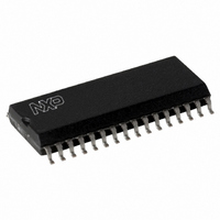
SLRC40001T/OFE,112 NXP Semiconductors, SLRC40001T/OFE,112 Datasheet - Page 90

SLRC40001T/OFE,112
Manufacturer Part Number
SLRC40001T/OFE,112
Description
IC I.CODE SLRC400 READER 32-SOIC
Manufacturer
NXP Semiconductors
Series
I-Coder
Datasheets
1.SLRC40001TOFE112.pdf
(130 pages)
2.SLRC40001TOFE112.pdf
(132 pages)
3.SLRC40001TOFE112.pdf
(101 pages)
Specifications of SLRC40001T/OFE,112
Rf Type
Read Only
Frequency
13.56MHz
Features
ISO15693, ISO18000-3
Package / Case
32-SOIC (0.300", 7.50mm Width)
Product
RFID Readers
Operating Temperature Range
- 25 C to + 85 C
Lead Free Status / RoHS Status
Lead free / RoHS Compliant
Lead Free Status / RoHS Status
Lead free / RoHS Compliant, Lead free / RoHS Compliant
Other names
568-1124-5
935269551112
SLRC400
SLRC41TOFED
935269551112
SLRC400
SLRC41TOFED
- Current page: 90 of 130
- Download datasheet (689Kb)
Philips Semiconductors
I•CODE Reader IC
14 RECEIVER CIRCUITRY
14.1 General
The SL RC400 employs an integrated quadrature-demodulation circuit which extracts the sub-carrier signal
from the 13.56 MHz ASK-modulated signal applied to pin RX. The quadrature-demodulator uses two
different clocks, Q- and I-clock, with a phase shift of 90° between them. Both resulting subcarrier signals are
amplified, filtered and forwarded to the correlation circuitry. The correlation results are evaluated, digitised
and passed to the digital circuitry.
For all processing units various adjustments can be made to obtain optimum performance.
14.2 Block Diagram
Figure 14-1 shows the block diagram of the receiver circuitry. The receiving process includes several steps.
First the quadrature demodulation of the carrier signal of 13.56 MHz is done. To achieve an optimum in
performance an automatic clock Q calibration is recommended (see 14.3.1). The demodulated signal is
amplified by an adjustable amplifier. A correlation circuit calculates the degree of similarity between the
expected and the received signal. The bit phase register allows to align the position of the correlation
intervals with the bit grid of the received signal. In the evaluation and digitizer circuitry the valid bits are
detected and the digital results are send to the FIFO register. Several tuning steps in this circuit are possible.
The user may observe the signal on its way through the receiver as shown in the block diagram above. One
signal at a time may be routed to pin AUX using the TestAnaSelect-Register as described in 18.3.
ClockQDelay[4:0]
RX
I-clock
Demodulator
Conversion
13.56 MHz
I to Q
ClockQCalib
Q-clock
VRxFollI
clock
ClockQ180°
VRxFollQ
Figure 14-1: Block Diagram of Receiver Circuitry
Gain[1:0]
VRxAmpI
VRxAmpQ
BitPhase[7:0]
Correlation
90
Circuitry
TestAna
OutSel
to
VCorrDI
Product Specification Rev. 3.1 August 2004
VCorrNI
VCorrDQ
VCorrNQ
MinLevel[3:0]
Evaluation and Digitizer
CollLevel[3:0]
VEvalR
Circuitry
RxWait[7:0]
VEvalL
SL RC400
RcvClkSelI
s_valid
s_data
s_coll
s_clock
Related parts for SLRC40001T/OFE,112
Image
Part Number
Description
Manufacturer
Datasheet
Request
R
Part Number:
Description:
NXP Semiconductors designed the LPC2420/2460 microcontroller around a 16-bit/32-bitARM7TDMI-S CPU core with real-time debug interfaces that include both JTAG andembedded trace
Manufacturer:
NXP Semiconductors
Datasheet:

Part Number:
Description:
NXP Semiconductors designed the LPC2458 microcontroller around a 16-bit/32-bitARM7TDMI-S CPU core with real-time debug interfaces that include both JTAG andembedded trace
Manufacturer:
NXP Semiconductors
Datasheet:
Part Number:
Description:
NXP Semiconductors designed the LPC2468 microcontroller around a 16-bit/32-bitARM7TDMI-S CPU core with real-time debug interfaces that include both JTAG andembedded trace
Manufacturer:
NXP Semiconductors
Datasheet:
Part Number:
Description:
NXP Semiconductors designed the LPC2470 microcontroller, powered by theARM7TDMI-S core, to be a highly integrated microcontroller for a wide range ofapplications that require advanced communications and high quality graphic displays
Manufacturer:
NXP Semiconductors
Datasheet:
Part Number:
Description:
NXP Semiconductors designed the LPC2478 microcontroller, powered by theARM7TDMI-S core, to be a highly integrated microcontroller for a wide range ofapplications that require advanced communications and high quality graphic displays
Manufacturer:
NXP Semiconductors
Datasheet:
Part Number:
Description:
The Philips Semiconductors XA (eXtended Architecture) family of 16-bit single-chip microcontrollers is powerful enough to easily handle the requirements of high performance embedded applications, yet inexpensive enough to compete in the market for hi
Manufacturer:
NXP Semiconductors
Datasheet:
Part Number:
Description:
The XA-S3 device is a member of Philips Semiconductors? XA(eXtended Architecture) family of high performance 16-bitsingle-chip microcontrollers
Manufacturer:
NXP Semiconductors
Datasheet:

Part Number:
Description:
The NXP BlueStreak LH75401/LH75411 family consists of two low-cost 16/32-bit System-on-Chip (SoC) devices
Manufacturer:
NXP Semiconductors
Datasheet:

Part Number:
Description:
The NXP LPC3130/3131 combine an 180 MHz ARM926EJ-S CPU core, high-speed USB2
Manufacturer:
NXP Semiconductors
Datasheet:

Part Number:
Description:
The NXP LPC3141 combine a 270 MHz ARM926EJ-S CPU core, High-speed USB 2
Manufacturer:
NXP Semiconductors

Part Number:
Description:
The NXP LPC3143 combine a 270 MHz ARM926EJ-S CPU core, High-speed USB 2
Manufacturer:
NXP Semiconductors

Part Number:
Description:
The NXP LPC3152 combines an 180 MHz ARM926EJ-S CPU core, High-speed USB 2
Manufacturer:
NXP Semiconductors

Part Number:
Description:
The NXP LPC3154 combines an 180 MHz ARM926EJ-S CPU core, High-speed USB 2
Manufacturer:
NXP Semiconductors

Part Number:
Description:
Standard level N-channel enhancement mode Field-Effect Transistor (FET) in a plastic package using NXP High-Performance Automotive (HPA) TrenchMOS technology
Manufacturer:
NXP Semiconductors
Datasheet:


