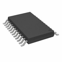
ADF7012BRUZ Analog Devices Inc, ADF7012BRUZ Datasheet - Page 23

ADF7012BRUZ
Manufacturer Part Number
ADF7012BRUZ
Description
IC XMITTER ASK/FSK/GFSK 24TSSOP
Manufacturer
Analog Devices Inc
Datasheet
1.EVAL-ADF7012EB1.pdf
(28 pages)
Specifications of ADF7012BRUZ
Frequency
75MHz ~ 1GHz
Applications
Data Transfer, RKE, Remote Control/Security Systems
Modulation Or Protocol
ASK, FSK, GFSK, OOK
Data Rate - Maximum
179.2 kbps
Power - Output
-16dBm ~ 14dBm
Current - Transmitting
35mA
Data Interface
PCB, Surface Mount
Antenna Connector
PCB, Surface Mount
Voltage - Supply
2.3 V ~ 3.6 V
Operating Temperature
-40°C ~ 85°C
Package / Case
24-TSSOP
Transmitting Current
16mA
Data Rate
179.2Kbps
Frequency Range
75MHz To 1GHz
Rf Ic Case Style
TSSOP
No. Of Pins
24
Supply Voltage Range
2.3V To 3.6V
Operating Temperature (min)
-40C
Operating Temperature (max)
85C
Operating Temperature Classification
Industrial
Product Depth (mm)
4.4mm
Operating Supply Voltage (min)
2.3V
Operating Supply Voltage (typ)
2.5/3.3V
Operating Supply Voltage (max)
3.6V
Lead Free Status / RoHS Status
Lead free / RoHS Compliant
For Use With
EVAL-ADF7012DBZ4 - BOARD EVALUATION DB4 FOR ADF7012EVAL-ADF7012DBZ3 - BOARD EVALUATION DB3 FOR ADF7012EVAL-ADF7012DBZ2 - BOARD EVALUATION DB2 FOR ADF7012EVAL-ADF7012DBZ1 - BOARD EVALUATION DB1 FOR ADF7012EVAL-ADF7012DBZ5 - BOARD DAUGHTER FOR ADF7012
Features
-
Memory Size
-
Lead Free Status / Rohs Status
Compliant
Available stocks
Company
Part Number
Manufacturer
Quantity
Price
Company:
Part Number:
ADF7012BRUZ
Manufacturer:
AD
Quantity:
9 458
Part Number:
ADF7012BRUZ
Manufacturer:
ADI/亚德诺
Quantity:
20 000
Part Number:
ADF7012BRUZ-RL
Manufacturer:
ADI/亚德诺
Quantity:
20 000
915 MHz OPERATION
The recommendations here are guidelines only. The design
should be subject to internal testing prior to FCC site testing.
Matching components need to be adjusted for board layout.
FCC 15.247 and FCC 15.249 are the main regulations governing
operation in the 902 MHz to 928 MHz Band. FCC 15.247
requires some form of spectral spreading. Typically, the
ADF7012 would be used in conjunction with the frequency
hopping spread spectrum (FHSS) or it may be used in
conjunction with the digital modulation standard which
requires large deviation frequencies. Output power of < 1 W
is tolerated on certain spreading conditions.
Compliance with FCC 15.249 limits the output power to
−1.5 dBm, but does not require spreading. There are many
different applications in this band, including remote controls
for security, sensor interrogation, metering, and home control.
Design Criteria
915.2MHz center frequency
FSK modulation
10 dBm output power
200 m range
Meets FCC 15.247
38.4 kbps data rate
The center frequency is 915.2 MHz. It is possible to operate
the VCO at this frequency. Figure 36 shows the inductor value
vs. center frequency. The inductor chosen is 1.6 nH. Coilcraft
inductors such as 0603-CS-1N6XJBU are recommended.
Additional hopping frequencies can easily be generated by
changing the N value.
Crystal and PFD
The phase noise requirement is such to ensure that the 20 dB
bandwidth requirements are met. These are dependent on the
channel spacing chosen. A typical channel spacing would be
400 kHz, which would allow 50 channels in 20 MHz and enable
the design to avoid the edges of the band.
The PFD is chosen to minimize spurious levels. There are beat
note spurious levels at 910 MHz and 920 MHz, but the level is
usually significantly less than the modulation power. They are
also attenuated quickly by the loop filter to ensure a quick
crystal power-up time.
PFD = 10 MHz − Power-Up Time 1.8 ms (approximately).
Figure 10 shows a typical power-on time for a 4 MHz crystal.
N-Divider
The N divider is determined as being:
Nint = 91
Nfrac = (2130)/4096
VCO divide-by-2 is not enabled
Rev. A | Page 23 of 28
Deviation
The deviation is set to ±19.2 kHz to accommodate a simple
receiver architecture, and to ensure the available spectrum is
used efficiently.
The modulation steps available are in 10 MHz/2
Bias Current
Because low current is desired, a 3 mA VCO bias can be used
and still ensure oscillation at 928 MHz. Additional bias current
reduces any spurious noise, but increases current consumption.
A 3 mA bias current gives the best spurious vs. phase noise
trade-off.
The PA bias should be set to 5.5 mA to achieve 10 dBm power.
Loop Filter Bandwidth
The loop filter is designed with the ADIsimSRD Design Studio.
A data rate of 170 kHz is chosen, which allows for data rates of
> 38.4 kbps. It also attenuates the beat note spurs quickly to
ensure they have no effect on system performance.
Design of Harmonic Filter
The main requirement of the harmonic filter should ensure
that the third harmonic level is < −41.5 dBm. A fifth-order
Chebyshev filter is recommended to achieve this, and a sug-
gested starting point is given next. The Pi format is chosen
to minimize the number of inductors in the system.
Component Values—Crystal: 10 MHz
Loop Filter
Icp
LBW
C1
C2
C3
R1
R2
Matching
L1
L2
C14
Harmonic Filter
L4
L5
C15
C16
C17
Modulation steps = 610 Hz
Modulation number = 19.2 kHz/610 Hz = 31.
1.44 mA
170 kHz
470 pF
12 nF
120 pF
470 Ω
1.8 kΩ
27 nH
6.2 nH
470 pF
8.2 nH
8.2 nH
4.7 pF
6.8 pF
4.7 pF
14
:
ADF7012


