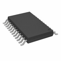
ADF7012BRUZ Analog Devices Inc, ADF7012BRUZ Datasheet - Page 14

ADF7012BRUZ
Manufacturer Part Number
ADF7012BRUZ
Description
IC XMITTER ASK/FSK/GFSK 24TSSOP
Manufacturer
Analog Devices Inc
Datasheet
1.EVAL-ADF7012EB1.pdf
(28 pages)
Specifications of ADF7012BRUZ
Frequency
75MHz ~ 1GHz
Applications
Data Transfer, RKE, Remote Control/Security Systems
Modulation Or Protocol
ASK, FSK, GFSK, OOK
Data Rate - Maximum
179.2 kbps
Power - Output
-16dBm ~ 14dBm
Current - Transmitting
35mA
Data Interface
PCB, Surface Mount
Antenna Connector
PCB, Surface Mount
Voltage - Supply
2.3 V ~ 3.6 V
Operating Temperature
-40°C ~ 85°C
Package / Case
24-TSSOP
Transmitting Current
16mA
Data Rate
179.2Kbps
Frequency Range
75MHz To 1GHz
Rf Ic Case Style
TSSOP
No. Of Pins
24
Supply Voltage Range
2.3V To 3.6V
Operating Temperature (min)
-40C
Operating Temperature (max)
85C
Operating Temperature Classification
Industrial
Product Depth (mm)
4.4mm
Operating Supply Voltage (min)
2.3V
Operating Supply Voltage (typ)
2.5/3.3V
Operating Supply Voltage (max)
3.6V
Lead Free Status / RoHS Status
Lead free / RoHS Compliant
For Use With
EVAL-ADF7012DBZ4 - BOARD EVALUATION DB4 FOR ADF7012EVAL-ADF7012DBZ3 - BOARD EVALUATION DB3 FOR ADF7012EVAL-ADF7012DBZ2 - BOARD EVALUATION DB2 FOR ADF7012EVAL-ADF7012DBZ1 - BOARD EVALUATION DB1 FOR ADF7012EVAL-ADF7012DBZ5 - BOARD DAUGHTER FOR ADF7012
Features
-
Memory Size
-
Lead Free Status / Rohs Status
Compliant
Available stocks
Company
Part Number
Manufacturer
Quantity
Price
Company:
Part Number:
ADF7012BRUZ
Manufacturer:
AD
Quantity:
9 458
Part Number:
ADF7012BRUZ
Manufacturer:
ADI/亚德诺
Quantity:
20 000
Part Number:
ADF7012BRUZ-RL
Manufacturer:
ADI/亚德诺
Quantity:
20 000
ADF7012
The deviation from the center frequency is set using the D1 to
D9 bits in the modulation register. The frequency deviation
may be set in steps of
The deviation frequency is therefore
where ModulationNumber is set by Bit D1 to Bit D9.
The maximum data rate is a function of the PLL lock time (and
the requirement on FSK spectrum). Because the PLL lock time
is reduced by increasing the loop-filter bandwidth, highest data
rates can be achieved for the wider loop filter bandwidths. The
absolute maximum limit on loop filter bandwidth to ensure
stability for a fractional-N PLL is F
frequency, the loop bandwidth could be as high as 2.85 MHz.
FSK modulation is selected by setting the S1 and S2 bits in the
modulation register low.
GFSK MODULATION
Gaussian frequency shift keying (GFSK) represents a filtered
form of frequency shift keying. The data to be modulated to
RF is prefiltered digitally using a finite impulse response filter
(FIR). The filtered data is then used to modulate the sigma-
delta fractional-N to generate spectrally-efficient FSK.
FSK consists of a series of sharp transitions in frequency as the
data is switched from one level to another. The sharp switching
generates higher frequency components at the output, resulting
in a wider output spectrum.
With GFSK, the sharp transitions are replaced with up to 128
smaller steps. The result is a gradual change in frequency. As a
result, the higher frequency components are reduced and the
spectrum occupied is reduced significantly. GFSK does require
some additional design work as the data is only sampled once
per bit, and so the choice of crystal is important to ensure the
correct sampling clock is generated.
FSK DEVIATION
TxDATA
FREQUENCY
–F
+F
F
F
DEV
DEV
STEP
DEVIATION
(
4R
Hz
)
(
=
Hz
CHARGE
F
FRACTIONAL-N
PUMP
Figure 30. FSK Implementation
2
)
PFD/
PFD
14
=
F
PFD
×
Σ-Δ MODULATOR
Modulation
THIRD-ORDER
PFD
2
14
/7. For a 20 MHz PFD
Number
INTEGER-N
VCO
÷N
PA STAGE
(5)
(6)
Rev. A | Page 14 of 28
For GFSK and GOOK, the incoming bit stream to be trans-
mitted needs to be synchronized with an on-chip sampling
clock which provides one sample per bit to the Gaussian FIR
filter. To facilitate this, the sampling clock is routed to the
TxCLK pin where data is fetched from the host microcontroller
or microprocessor on the falling edge of TxCLK, and the data
is sampled at the midpoint of each bit on TxCLK’s rising edge.
Inserting external RC LPFs on TxDATA and TxCLK lines
creates smoother edge transitions and improves spurious
performance. As an example, suitable components are a 1 kΩ
resistor and a 10 nF capacitor for a data rate of 5 kbps.
The number of steps between symbol 0 and symbol 1 is
determined by the setting for the index counter.
The GFSK deviation is set up as
where m is the mod control (Bit MC1 to Bit MC3 in the
modulation register).
The GFSK sampling clock samples data at the data rate
where the DividerFactor is set by Bit D1 to Bit D7, and the
IndexCounter is set by Bit IC1 and Bit IC2 in the modulation
register.
POWER AMPLIFIER
The output stage is based on a Class E amplifier design, with
an open-drain output switched by the VCO signal. The output
control consists of six current mirrors operating as a program-
mable current source.
To achieve maximum voltage swing, the RF
biased at DV
current supply to the output stage; PA is biased to DV
and with the correct choice of value transforms the impedance.
The output power can be adjusted by changing the value of
Bit P1 to Bit P6. Typically, this is P1 to P6 output −20dBm at
0x0, and 13 dBm at 0x7E at 868 MHz, with the optimum
matching network.
μC
GFSK
DataRate
INT
I/O
DEVIATION
DD
Figure 31. TxCLK/TxDATA Synchronization.
. A single pull-up inductor to DV
FETCH
(
bps
SAMPLE
)
(
Hz
=
FETCH
DividerFac
)
=
SAMPLE
F
PFD
FETCH
2
12
×
SAMPLE
2
tor
m
F
PFD
×
FETCH
IndexCount
OUT
pin needs to be
DD
ensures a
TxDATA
TxCLK
ADF7012
er
DD
volts,
(7)
(8)


