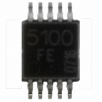
TDK5100F Infineon Technologies, TDK5100F Datasheet - Page 15

TDK5100F
Manufacturer Part Number
TDK5100F
Description
TRANSMITTER ASK/FSK SGL TSSOP10
Manufacturer
Infineon Technologies
Type
Transmitterr
Datasheet
1.TDK5100F.pdf
(39 pages)
Specifications of TDK5100F
Package / Case
10-TSSOP
Frequency
434MHz Center
Applications
Alarm Systems, Communication Systems
Modulation Or Protocol
ASK, FSK
Data Rate - Maximum
20 kbps
Power - Output
3.2dBm
Current - Transmitting
7mA
Data Interface
PCB, Surface Mount
Antenna Connector
PCB, Surface Mount
Voltage - Supply
2.1 V ~ 4 V
Operating Temperature
-25°C ~ 85°C
Operating Frequency
435 MHz
Operating Supply Voltage
2.5 V, 3.3 V
Maximum Operating Temperature
+ 125 C
Minimum Operating Temperature
- 40 C
Mounting Style
SMD/SMT
Operating Temperature (min)
-40C
Operating Temperature (max)
125C
Operating Temperature Classification
Automotive
Operating Supply Voltage (min)
2.1V
Operating Supply Voltage (typ)
2.5/3.3V
Lead Free Status / RoHS Status
Lead free / RoHS Compliant
Features
-
Memory Size
-
Lead Free Status / Rohs Status
Compliant
Other names
SP000014745
TDK5100F
TDK5100FINTR
TDK5100FXT
TDK5100F
TDK5100FINTR
TDK5100FXT
Available stocks
Company
Part Number
Manufacturer
Quantity
Price
Company:
Part Number:
TDK5100F
Manufacturer:
ST
Quantity:
2 100
Company:
Part Number:
TDK5100F
Manufacturer:
Infineon Technologies
Quantity:
135
Part Number:
TDK5100F
Manufacturer:
INFINEON/英飞凌
Quantity:
20 000
Part Number:
TDK5100FHTMA1
Manufacturer:
INFINEON/英飞凌
Quantity:
20 000
2.4.4.3
In the TRANSMIT MODE the PLL is switched on and the power amplifier is turned on too.
The current consumption of the IC is typically 7 mA when using a proper transforming
network at PAOUT, see Figure 8.
2.4.4.4
The bias circuitry is powered up via a voltage V > 1.5 V at the pin PDWN (pin10).
When the bias circuitry is powered up, the pins ASKDTA and FSKDTA are pulled up
internally.
Forcing the voltage at the pins low overrides the internally set state.
Alternatively, if the voltage at ASKDTA or FSKDTA is forced high externally, the PDWN
pin is pulled up internally via a current source. In this case, it is not necessary to connect
the PDWN pin, it is recommended to leave it open.
The principle schematic of the power mode control circuitry is shown in Figure 3
Figure 3
Data Sheet
ASKDTA
FSKDTA
PDWN
Transmit Mode
Power mode control
Power mode control circuitry
Source
Bias
On
120 kΩ
120 kΩ
PLL
MHz
434
15
PA
OR
On
FSK
IC
Functional Description
V 1.2, 2008-04-04
TDK5100F
FSKOUT
PAOUT


