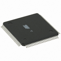
ATMEGA128RZBV-8AU Atmel, ATMEGA128RZBV-8AU Datasheet - Page 58

ATMEGA128RZBV-8AU
Manufacturer Part Number
ATMEGA128RZBV-8AU
Description
MCU ATMEGA1280/AT86RF230 100TQFP
Manufacturer
Atmel
Series
ATMEGAr
Datasheets
1.ATMEGA640V-8CU.pdf
(38 pages)
2.ATMEGA640V-8CU.pdf
(444 pages)
3.AT86RF230-ZU.pdf
(98 pages)
Specifications of ATMEGA128RZBV-8AU
Frequency
2.4GHz
Data Rate - Maximum
2Mbps
Modulation Or Protocol
802.15.4 Zigbee
Applications
General Purpose
Power - Output
3dBm
Sensitivity
-101dBm
Voltage - Supply
1.8 V ~ 3.6 V
Data Interface
PCB, Surface Mount
Memory Size
128kB Flash, 4kB EEPROM, 8kB RAM
Antenna Connector
PCB, Surface Mount
Package / Case
100-TQFP
Wireless Frequency
2.4 GHz
Interface Type
JTAG, SPI
Output Power
3 dBm
For Use With
ATAVRISP2 - PROGRAMMER AVR IN SYSTEMATSTK501 - ADAPTER KIT FOR 64PIN AVR MCUATSTK500 - PROGRAMMER AVR STARTER KIT
Lead Free Status / RoHS Status
Lead free / RoHS Compliant
Operating Temperature
-
Current - Transmitting
-
Current - Receiving
-
Lead Free Status / Rohs Status
Lead free / RoHS Compliant
For Use With/related Products
ATmega128
9 Module Description
9.1 Receiver (RX)
9.1.1 Overview
9.1.2 Configuration
9.2 Transmitter (TX)
9.2.1 Overview
58
AT86RF230
The AT86RF230 receiver is spitted into an analog radio front end and a digital base
band processor (RX BBP), see Figure 3-1.
The RF signal is amplified by a low noise amplifier (LNA) and converted down to an
intermediate frequency by a mixer. Channel selectivity is performed using an integrated
band pass filter. A limiting amplifier (Limiter) provides sufficient gain to overcome the
DC offset of the succeeding analog-to-digital converter (ADC) and generates a digital
RSSI signal with 3 dB granularity. The IF signal is sampled and processed further by
the digital base band receiver.
The RX BBP performs additional signal filtering and signal synchronization. The
frequency offset of each frame is calculated by the synchronization unit and is used
during the remaining receive process to correct the offset. The receiver is designed to
handle frequency and symbol rate deviations up to ±120 ppm, caused by combined
receiver and transmitter deviations. For details refer to section 11.5 parameter 11.5.6.
Finally the signal is demodulated and the data are stored to the Frame Buffer.
In Basic Operating Mode the start of an IEEE 802.15.4 compliant frame is indicated by
a RX_START interrupt. Accordingly it’s end is signalized by an TRX_END interrupt.
Based on the quality of the received signal a link quality indicator (LQI) is calculated
and appended to the frame, refer to section 8.5. Additional signal processing is applied
to the frame data to provide further status information like ED value (register 0x07) and
FCS correctness (register 0x06).
Beyond these features the Extended Operating Mode of the AT86RF230 supports
address filtering and pending data indication. For details refer to section 7.2.
The receiver is enabled by writing the command RX_ON for the Basic Operating Mode
or RX_AACK_ON for the Extended Operating Mode to register bits TRX_CMD in
register 0x02 (TRX_STATE).
The receiver does not need any additional configuration to receive IEEE 802.15.4
compliant frames on the current selected channel when using the Basic Operating
Mode. However the frame reception in the Extended Operating Mode requires further
register configurations, for details refer to section 7.2.
The AT86RF230 transmitter consists of a digital base band processor (TX BBP) and an
analog radio front end, see Figure 3-1.
The TX BBP reads the frame data from the Frame Buffer and performs the bit-to-
symbol and symbol-to-chip mapping as specified by IEEE 802.15.4 in section 6.5.2.
The O-QPSK modulation signal is generated and fed into the analog radio front end.
The fractional-N frequency synthesizer (PLL) converts the baseband transmit signal to
the RF signal, which is amplified by the power amplifier (PA). The PA output is internally
5131E-MCU Wireless-02/09


