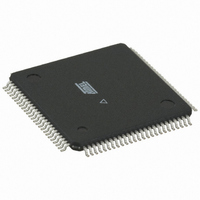
ATMEGA128RZBV-8AU Atmel, ATMEGA128RZBV-8AU Datasheet - Page 3

ATMEGA128RZBV-8AU
Manufacturer Part Number
ATMEGA128RZBV-8AU
Description
MCU ATMEGA1280/AT86RF230 100TQFP
Manufacturer
Atmel
Series
ATMEGAr
Datasheets
1.ATMEGA640V-8CU.pdf
(38 pages)
2.ATMEGA640V-8CU.pdf
(444 pages)
3.AT86RF230-ZU.pdf
(98 pages)
Specifications of ATMEGA128RZBV-8AU
Frequency
2.4GHz
Data Rate - Maximum
2Mbps
Modulation Or Protocol
802.15.4 Zigbee
Applications
General Purpose
Power - Output
3dBm
Sensitivity
-101dBm
Voltage - Supply
1.8 V ~ 3.6 V
Data Interface
PCB, Surface Mount
Memory Size
128kB Flash, 4kB EEPROM, 8kB RAM
Antenna Connector
PCB, Surface Mount
Package / Case
100-TQFP
Wireless Frequency
2.4 GHz
Interface Type
JTAG, SPI
Output Power
3 dBm
For Use With
ATAVRISP2 - PROGRAMMER AVR IN SYSTEMATSTK501 - ADAPTER KIT FOR 64PIN AVR MCUATSTK500 - PROGRAMMER AVR STARTER KIT
Lead Free Status / RoHS Status
Lead free / RoHS Compliant
Operating Temperature
-
Current - Transmitting
-
Current - Receiving
-
Lead Free Status / Rohs Status
Lead free / RoHS Compliant
For Use With/related Products
ATmega128
3 General Circuit Description
Figure 3-1. Block Diagram of the AT86RF230
5131E-MCU Wireless-02/09
RFP
RFN
LNA
BATMON
AVREG
FTN
PPF
Q
I
Analog Domain
This single-chip radio transceiver provides a complete radio transceiver interface
between the antenna and the microcontroller. It comprises the analog radio transceiver
and the digital demodulation including time and frequency synchronization, and data
buffering. The number of external components is minimized such that only an antenna,
a crystal and four decoupling capacitors are required. The bidirectional differential
antenna pins are used for transmission and reception, so that no external antenna
switch is needed.
The AT86RF230 block diagram is shown in Figure 3-1.
The received RF signal at pins RFN and RFP is differentially fed through the low-noise
amplifier (LNA) to the RF filter (PPF) to generate a complex signal. This signal is
converted down by mixers to an intermediate frequency and fed to the integrated
channel filter (SSBF). The limiting amplifier provides sufficient gain to drive the
succeeding analog-to-digital converter (ADC) and generates a digital RSSI signal with
3 dB granularity. The ADC output signal is sampled by the digital base band receiver
(RX BBP).
The transmit modulation scheme is offset-QPSK (O-QPSK) with half-sine pulse shaping
and 32-length block coding (spreading) according to [1]. The modulation signal is
generated in the digital transmitter (TX BBP) and applied to the fractional-N frequency
synthesis (PLL) generating a coherent phase modulation required for demodulation of
O-QPSK signals. The frequency-modulated RF signal is fed to the power amplifier (PA).
An internal 128 byte RAM for RX and TX (Frame Buffer) buffers the data to be
transmitted or the received data. Two on chip low dropout (LDO) voltage regulators
provide the internal analog and digital 1.8V supply.
TX power
control
PA
SSBF
Limiter
AGC
Frequency
Synthesis
RSSI
XOSC
ADC
5
TX Data
DCLK
RX BBP
TX BBP
Control Logic/
Configuration
Registers
Digital Domain
Buffer
Fame
AT86RF230
Interface
DVREG
Slave
SPI
SLP_TR
CLKM
RST
MISO
SCLK
MOSI
IRQ
SEL
3


