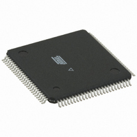
ATMEGA128RZBV-8AU Atmel, ATMEGA128RZBV-8AU Datasheet - Page 5

ATMEGA128RZBV-8AU
Manufacturer Part Number
ATMEGA128RZBV-8AU
Description
MCU ATMEGA1280/AT86RF230 100TQFP
Manufacturer
Atmel
Series
ATMEGAr
Datasheets
1.ATMEGA640V-8CU.pdf
(38 pages)
2.ATMEGA640V-8CU.pdf
(444 pages)
3.AT86RF230-ZU.pdf
(98 pages)
Specifications of ATMEGA128RZBV-8AU
Frequency
2.4GHz
Data Rate - Maximum
2Mbps
Modulation Or Protocol
802.15.4 Zigbee
Applications
General Purpose
Power - Output
3dBm
Sensitivity
-101dBm
Voltage - Supply
1.8 V ~ 3.6 V
Data Interface
PCB, Surface Mount
Memory Size
128kB Flash, 4kB EEPROM, 8kB RAM
Antenna Connector
PCB, Surface Mount
Package / Case
100-TQFP
Wireless Frequency
2.4 GHz
Interface Type
JTAG, SPI
Output Power
3 dBm
For Use With
ATAVRISP2 - PROGRAMMER AVR IN SYSTEMATSTK501 - ADAPTER KIT FOR 64PIN AVR MCUATSTK500 - PROGRAMMER AVR STARTER KIT
Lead Free Status / RoHS Status
Lead free / RoHS Compliant
Operating Temperature
-
Current - Transmitting
-
Current - Receiving
-
Lead Free Status / Rohs Status
Lead free / RoHS Compliant
For Use With/related Products
ATmega128
4.2 Analog and RF Pins
5131E-MCU Wireless-02/09
AVDD, DVDD
AVDD and DVDD are outputs of the internal 1.8V voltage regulators. The voltage
regulators are controlled independently by the radio transceivers state machine and are
activated depending on the current radio transceiver state. The voltage regulators can
be configured for external supply. For details refer to section 9.4.
AVSS, DVSS
AVSS and DVSS are analog and digital ground pins respectively.
The analog and digital power domains should be separated on the PCB, for further
details see application note AVR2005 "Design Considerations for the AT86RF230".
RFP, RFN
A differential RF port (RFP/RFN) provides common-mode rejection to suppress the
switching noise of the internal digital signal processing blocks. At the board-level, the
differential RF layout ensures high receiver sensitivity by rejecting any spurious
interspersions originating from other digital ICs such as a microcontroller.
The RF port is designed for a 100Ω differential load. A DC path between the RF pins is
allowed. A DC path to ground or supply voltage is not allowed. Therefore, when
connecting a RF-load providing a DC path to the power supply or to ground, capacitive
coupling is required as indicated in Table 4-2.
A simplified schematic of the RF front end is shown in Figure 4-1.
Figure 4-1. Simplified RF Front-End Schematic
RF port DC values depend on the operating mode. In TRX_OFF state (see section
7.1.2), when the analog front end is disabled, the RF pins are pulled to ground,
preventing a floating voltage.
RFN
RFP
PCB
AT86RF230
M0
0.9V
RXTX
CM
Feedback
LNA
PA
RX
TX
AT86RF230
5


