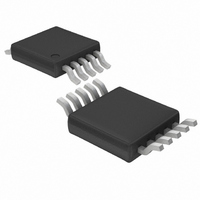
LTC1757A-2EMS Linear Technology, LTC1757A-2EMS Datasheet - Page 8

LTC1757A-2EMS
Manufacturer Part Number
LTC1757A-2EMS
Description
IC CTRLR RF POWER DUAL 10MSOP
Manufacturer
Linear Technology
Datasheet
1.LTC1757A-1EMS8.pdf
(16 pages)
Specifications of LTC1757A-2EMS
Rf Type
Cellular, GSM, PCS, Wireless Modem, TDMA
Frequency
850MHz ~ 2GHz
Features
Dual Output
Package / Case
10-MSOP, Micro10™, 10-uMAX, 10-uSOP
Lead Free Status / RoHS Status
Contains lead / RoHS non-compliant
Available stocks
Company
Part Number
Manufacturer
Quantity
Price
Company:
Part Number:
LTC1757A-2EMS
Manufacturer:
LT
Quantity:
10 000
Part Number:
LTC1757A-2EMS
Manufacturer:
LT
Quantity:
20 000
Company:
Part Number:
LTC1757A-2EMS#TR
Manufacturer:
LT
Quantity:
2 817
Company:
Part Number:
LTC1757A-2EMS#TRPBF
Manufacturer:
AMD
Quantity:
6 221
Part Number:
LTC1757A-2EMS#TRPBF
Manufacturer:
LT/凌特
Quantity:
20 000
APPLICATIO S I FOR ATIO
LTC1757A-1/LTC1757A-2
External Termination
The LTC1757A has an internal 185 termination resistor
at the RF pin. If a directional coupler is used, it is
recommended that an external 68 termination resistor
be connected between the RF coupling capacitor (33pF),
and ground at the side connected to the directional
coupler. If the termination is placed at the LTC1757A RF
pin, then the 68 resistor must be connected to V
the detector is referenced to V
nents should be placed adjacent to the LTC1757A.
Power Ramp Profiles
The external voltage gain associated with the RF channel
can vary significantly between RF power amplifier types.
The LTC1757A frequency compensation has been opti-
mized to be stable with several different power amplifiers
and manufacturers. This frequency compensation gener-
ally defines the loop dynamics that impact the power/time
response and possibly (slow loops) the power ramp
sidebands. The LTC1757A operates open loop until an RF
voltage appears at the RF pin, at which time the loop
8
U
U
IN
SHDN
TXEN
–10
–20
–30
–40
–50
–60
–70
–80
. Termination compo-
10
W
0
START
100mV
CODE
–28
START
PULSE
Figure 1. LTC1757A Ramp Timing
50 s MINIMUM, ALLOWS TIME FOR DAC
AND AUTOZERO TO SETTLE
U
–18
IN
–10
since
0
TIME ( s)
closes and the output power follows the DAC profile. The
RF power amplifier will require a certain control voltage
level (threshold) before an RF output signal is produced.
The LTC1757A V
threshold voltage in order to meet the power/time profile.
To reduce this time, the LTC1757A starts at 550mV.
However, at very low power levels the PCTL input signal is
small, and the V
onds to reach the RF power amplifier threshold voltage. To
reduce this time, it may be necessary to apply a positive
pulse at the start of the ramp to quickly bring the V
outputs to the threshold voltage. This can generally be
achieved with DAC programming. The magnitude of the
pulse is dependent on the RF amplifier characteristics.
Power ramp sidebands and power/time are also a factor
when ramping to zero power. For RF amplifiers requiring
high control voltages, it may be necessary to further adjust
the DAC ramp profile. When the power is ramped down the
loop will eventually open at power levels below the
LTC1757A detector threshold. The LTC1757A will then go
open loop and the output voltage at V
543
553
561
PCA/B
PCA/B
571
outputs may take several microsec-
ZERO
CODE
outputs must quickly rise to this
1757A F01
PCA
or V
PCB
will stop
PCA/B


