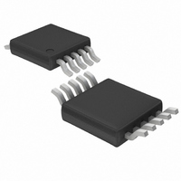
LTC1757A-2EMS Linear Technology, LTC1757A-2EMS Datasheet - Page 6

LTC1757A-2EMS
Manufacturer Part Number
LTC1757A-2EMS
Description
IC CTRLR RF POWER DUAL 10MSOP
Manufacturer
Linear Technology
Datasheet
1.LTC1757A-1EMS8.pdf
(16 pages)
Specifications of LTC1757A-2EMS
Rf Type
Cellular, GSM, PCS, Wireless Modem, TDMA
Frequency
850MHz ~ 2GHz
Features
Dual Output
Package / Case
10-MSOP, Micro10™, 10-uMAX, 10-uSOP
Lead Free Status / RoHS Status
Contains lead / RoHS non-compliant
Available stocks
Company
Part Number
Manufacturer
Quantity
Price
Company:
Part Number:
LTC1757A-2EMS
Manufacturer:
LT
Quantity:
10 000
Part Number:
LTC1757A-2EMS
Manufacturer:
LT
Quantity:
20 000
Company:
Part Number:
LTC1757A-2EMS#TR
Manufacturer:
LT
Quantity:
2 817
Company:
Part Number:
LTC1757A-2EMS#TRPBF
Manufacturer:
AMD
Quantity:
6 221
Part Number:
LTC1757A-2EMS#TRPBF
Manufacturer:
LT/凌特
Quantity:
20 000
APPLICATIO S I FOR ATIO
LTC1757A-1/LTC1757A-2
Operation
The LTC1757A-2 dual band RF power control amplifier
integrates several functions to provide RF power control
over two frequencies ranging from 850MHz to 2GHz. The
device also prevents damage to the RF power amplifier
due to overvoltage or overcurrent conditions. These func-
tions include an internally compensated power control
amplifier to control the RF output power, an autozero
section to cancel internal and external voltage offsets, a
sense amplifier with an internal sense resistor to limit the
maximum RF power amplifier current, an RF Schottky
diode peak detector and amplifier to convert the RF feed-
back signal to DC, a V
overvoltage detector, a bandgap reference, a thermal
shutdown circuit and a multiplexer to switch the control
amplifier output to either V
Band Selection
The LTC1757A-2 is designed for dual band operation. The
BSEL pin will select output V
when high. For example, V
900MHz channel and V
BSEL must be established before the part is enabled. The
LTC1757A-1 can be used to drive a single RF channel or
dual channel module with integral multiplexer.
Control Amplifier
The control amplifier supplies the power control voltage to
the RF power amplifier. A portion (typically – 19dB for low
frequencies and –14dB for high frequencies) of the RF
output signal is sampled, via a directional coupler, to close
the gain control loop. When a DAC signal is applied to
PCTL, the amplifier quickly servos V
until the detected feedback voltage applied to the RF pin
matches the voltage at PCTL. This feedback loop provides
accurate RF power control. V
driving a 5.5mA load current and 100pF load capacitor.
RF Detector
The internal RF Schottky diode peak detector and ampli-
fier converts the RF feedback voltage from the directional
coupler to a low frequency voltage. This voltage is com-
pared to the DAC voltage at the PCTL pin by the control
6
U
PCA/B
PCB
U
PCA
PCA
PCA
a 1.8GHz/1.9GHz channel.
PCA
overvoltage clamp, a V
or V
when low and output V
could be used to drive a
or V
W
PCB
PCA
PCB
.
or V
are capable of
PCB
U
positive
PCB
IN
amplifier to close the RF power control loop. The RF pin
input resistance is typically 185
range of this pin is 850MHz to 2000MHz. The detector
demonstrates excellent efficiency and linearity over a
wide range of input power. The Schottky detector is biased
at about 60 A and drives an on-chip peak detector capaci-
tor of 22pF.
Autozero
An autozero system is included to improve power pro-
gramming accuracy over temperature. This section can-
cels internal offsets associated with the Schottky diode
detector and control amplifier. External offsets associated
with the DAC driving the PCTL pin are also cancelled.
Offset drift due to temperature is cancelled between each
burst by the autozero system. The maximum offset al-
lowed at the DAC output is limited to 400mV. Autozeroing
is performed when the part is in autozero mode (SHDN =
high, TXEN = low). When the part is enabled (TXEN = high,
SHDN = high) the autozero capacitors are held and the
V
output. The hold droop voltage of typically 10 V/ms
provides for accurate offset cancellation over the 1/8 duty
cycle associated with the GSM protocol as well as multislot
protocals. The part must be in the autozero mode for at
least 50 s for autozero to settle to the correct value.
Protection Features
The RF power amplifier is overcurrent protected by an
internal sense amplifier. The sense amplifier measures the
voltage across an internal 0.050 resistor to determine
the RF power amplifier current. V
this supply current exceeds 2.2A, thereby regulating the
current to about 2.25A. The regulated current limit is
temperature compensated. The 0.050 resistor and the
current limit feature can be removed by connecting the PA
directly to V
The RF power amplifier control voltage pins are overvolt-
age protected. The V
or V
tion attempts to exceed this voltage.
The RF power amplifier is protected against excessive
input supply voltages. The V
PCA
PCB
or V
to 2.85V when the gain and PCTL input combina-
PCB
IN
.
pin is connected to the control amplifier
PC
overvoltage clamp regulates V
IN
overvoltage detector starts
PCA
or V
and the frequency
PCB
is lowered as
PCA


