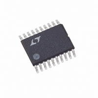
LT5503EFE#TR Linear Technology, LT5503EFE#TR Datasheet - Page 15

LT5503EFE#TR
Manufacturer Part Number
LT5503EFE#TR
Description
IC DIRECT IQ MOD/MIXER 20-TSSOP
Manufacturer
Linear Technology
Datasheet
1.LT5503EFE.pdf
(20 pages)
Specifications of LT5503EFE#TR
Function
Modulator/Mixer
Lo Frequency
1.4GHz ~ 2.4GHz
Rf Frequency
1.7GHz ~ 2.7GHz
P1db
-15dBm
Noise Floor
-152dBm/Hz
Output Power
12.7dBm
Current - Supply
38mA
Voltage - Supply
1.8 V ~ 5.25 V
Test Frequency
2.4GHz
Package / Case
20-TSSOP Exposed Pad, 20-eTSSOP, 20-HTSSOP
Pin Count
20
Screening Level
Industrial
Lead Free Status / RoHS Status
Contains lead / RoHS non-compliant
Other names
LT5503EFETR
Available stocks
Company
Part Number
Manufacturer
Quantity
Price
APPLICATIO S I FOR ATIO
Pin 16 should be connected externally to V
low value series resistor (47Ω typical). To assure proper
output power control, a good, local high frequency AC
ground for Pin 16 is essential. The MODOUT port of the
VGA is an open collector configuration. An inductor with
high self resonance frequency is required to connect
Pin 17 to V
output matching network. Additional matching compo-
nents are required to drive a 50Ω load as shown in
Figure 1. The amplifier is designed to operate in Class A for
low distortion performance. The typical output 1dB com-
pression point (P1dB) is –3dBm at 2.45GHz. When the
differential baseband input voltages are higher than 1V
the VGA operates in Class AB mode, and the distortion
performance of the modulator is degraded. The logic
control inputs do not draw current when they are low. They
draw about 2μA each when high.
Mixer LO1 Port
The mixer LO1 input port is the linear input to the mixer.
It consists of an active balun amplifier designed to operate
over the 1.4GHz to 2.4GHz frequency range. There is a
linear relationship between LO1 input power and
MIXRFOUT power for LO1 input levels up to approximately
–20dBm. After that, the mixer output begins to compress.
When operated in the recommended –14dBm to –8dBm
input power range, the mixer is well compressed, which in
turn creates a stable output level for the modulator input.
As shown in Figure 1, a simple lowpass matching network
is required to match this pin to 50Ω. This pin is internally
biased, therefore an AC-coupling capacitor is required.
MIXRFOUT
C5
CC
MX
as a DC return path, and as a part of the
+
10
L5
U
C9
LB
+
U
V
CC
R
C
51Ω
BYPASS
TERM
LB
–
W
Figure 5. 50Ω Mixer Output Matching Without a Balun
11
L6
MX
–
5503 F05
CC
C6
U
through a
P-P
,
Mixer LO2 Port
The mixer LO2 port is designed to operate in the 50MHz to
1000MHz range. The first stage is a limiting amplifier. This
stage produces the correct output levels to drive the
internal divider circuit reliably, with LO2 input levels down
to –20dBm. The output of the divider then drives another
stage, which in turn switches the nonlinear inputs of the
double-balanced mixer. Note that the mixer output will
produce broadband noise if the LO2 signal level is too low.
The input amplifier is designed for a good match over the
entire frequency range. The only requirement (Figure 1) is
an external AC-coupling capacitor.
Mixer Output Ports (MX
The mixer output is a differential open collector configura-
tion. Bias current is supplied to these two pins through the
center tap of a balun as shown in Figure 1. Simple lowpass
matching is used to transform each leg of the mixer output
to 25Ω for the balun’s 50Ω input impedance.
The balun approach provides the highest output power
and best LO1 suppression, but is not absolutely neces-
sary. It is also possible to match each output to 50Ω and
couple power from one output. The unused output should
be terminated in the same characteristic impedance. In
this case, output power is approximately 2dB lower and
LO1 suppression degrades to approximately 15dBc. A
schematic for this approach is shown in Figure 6 where
inductors LB
differential outputs, and resistor R
unused output.
L5,L6
C5, C6
C9
+
and LB
1.9GHz
5.6nH
1.8pF
–
15pF
supply bias current to the mixer’s
+
/MX
–
)
TERM
terminates the
LT5503
2.4GHz
0.68pF
2.7nH
8.2pF
15
5503f


