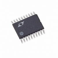
LT5503EFE#TR Linear Technology, LT5503EFE#TR Datasheet - Page 14

LT5503EFE#TR
Manufacturer Part Number
LT5503EFE#TR
Description
IC DIRECT IQ MOD/MIXER 20-TSSOP
Manufacturer
Linear Technology
Datasheet
1.LT5503EFE.pdf
(20 pages)
Specifications of LT5503EFE#TR
Function
Modulator/Mixer
Lo Frequency
1.4GHz ~ 2.4GHz
Rf Frequency
1.7GHz ~ 2.7GHz
P1db
-15dBm
Noise Floor
-152dBm/Hz
Output Power
12.7dBm
Current - Supply
38mA
Voltage - Supply
1.8 V ~ 5.25 V
Test Frequency
2.4GHz
Package / Case
20-TSSOP Exposed Pad, 20-eTSSOP, 20-HTSSOP
Pin Count
20
Screening Level
Industrial
Lead Free Status / RoHS Status
Contains lead / RoHS non-compliant
Other names
LT5503EFETR
Available stocks
Company
Part Number
Manufacturer
Quantity
Price
LT5503
APPLICATIO S I FOR ATIO
AC-Coupled Baseband . Figure 3 shows the simplified
circuit schematic of a high-pass AC-coupled baseband
interface.
With approximately 18k of differential input resistance,
the suggested minimum AC-coupling capacitor can be
determined using the following equation:
where f
signal.
A larger capacitor may be used where the settling time of
charging and discharging the AC-coupling capacitor is not
critical.
DC-Coupled Baseband . The baseband inputs’ internal bias
voltage can be overdriven with an external bias circuit.
This facilitates direct interfacing to a D/A converter for
faster transient response. In this case, the LT5503’s
baseband inputs are DC biased by the converter. The
optimal V
maximum V
load on each converter output can be approximated using
the following equation where I
into a modulator input:
14
I
C
INPUT
CPL
C
is the 3dB cut-off frequency of the baseband input
=
BIAS
=
Figure 3. AC-Coupled Baseband Interface
( •
18 10
Q
BIAS
V
I
Q
B
B
I
BIAS
is 1.4V, independent of V
C
C
C
C
9
should be less than V
CPL
CPL
CPL
CPL
k
−
3
Ω
1
U
1 4
• • )
.
π
BQ
BQ
V
BI
BI
+
–
+
–
f
C
U
LT5503
INPUT
18k
18k
0.8pF
0.8pF
0.8pF
0.8pF
W
is the current flowing
CC
CC
5505 F03
. In general, the
– 0.4V. The DC
U
Figure 4 shows a simplified circuit schematic for interfac-
ing the LT5503’s baseband inputs to the outputs of a D/A
converter. OIP and OIN are the positive and negative
baseband outputs, respectively, of the converter’s
I-channel. Similarly, OQP and OQN are the positive and
negative baseband outputs, respectively, of the converter’s
Q-channel.
Modulator RF Input (MODRFIN)
The modulator RF input buffer is driven single-ended. An
internal active balun circuit produces balanced signals to
drive the integrated phase shifter. Limiters following the
phase shifter output accommodate a wide range of
MODRFIN power, resulting in minimal degradation of
modulation gain/phase accuracy performance or carrier
feedthrough. This pin is easily matched to a 50Ω source
with the simple lowpass network shown in Figure 1. This
pin is internally biased, therefore an AC-coupling capaci-
tor is required.
Modulator VGA (Variable Gain Amp)
The VGA has two digital selection lines to provide a
nominal 0dB, 4.5dB, 9dB and 13.5dB attenuation from the
maximum modulator output power setting. The logic table
is shown below:
GC1
Attenuation
Figure 4. DC-Coupled Baseband Interface
D/A
OQP
OQN
OIN
OIP
High
Low
I
I
I
I
INPUT
INPUT
INPUT
INPUT
BQ
BQ
BI
BI
+
–
+
–
LT5503
4.5dB
Low
0dB
18k
18k
0.8pF
0.8pF
0.8pF
0.8pF
GC2
5505 F04
13.5dB
High
9dB
5503f


