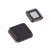
ADL5374ACPZ-R7 Analog Devices Inc, ADL5374ACPZ-R7 Datasheet - Page 15

ADL5374ACPZ-R7
Manufacturer Part Number
ADL5374ACPZ-R7
Description
IC MOD QUAD 3000-4000MHZ 24LFCSP
Manufacturer
Analog Devices Inc
Datasheet
1.ADL5374ACPZ-R7.pdf
(20 pages)
Specifications of ADL5374ACPZ-R7
Design Resources
Interfacing ADL5374 to AD9779A Dual-Channel, 1 GSPS High Speed DAC (CN0020)
Function
Modulator
Lo Frequency
2.8GHz ~ 4GHz
Rf Frequency
2.8GHz ~ 4GHz
P1db
12dBm
Noise Floor
-159.7dBm/Hz
Output Power
5dBm
Current - Supply
175mA
Voltage - Supply
4.75 V ~ 5.25 V
Test Frequency
3.8GHz
Package / Case
24-VFQFN, 24-CSP Exposed Pad
Frequency Range
3000MHz To 4000MHz
Rf Type
Quadrature
Supply Voltage Range
4.75V To 5.25V
Rf Ic Case Style
LFCSP
No. Of Pins
24
Operating Temperature Range
-40°C To +85°C
Lead Free Status / RoHS Status
Lead free / RoHS Compliant
Other names
ADL5374ACPZ-R7TR
An example is shown in Figure 32 with a third-order, Bessel
low-pass filter with a 3 dB frequency of 10 MHz. Matching input
and output impedances makes the filter design easier, so the
shunt resistor chosen is 100 Ω, producing an ac swing of
1 V p-p differential. The frequency response of this filter is
shown in Figure 33.
USING THE AD9779 AUXILIARY DAC FOR CARRIER
FEEDTHROUGH NULLING
The
inject small currents into the differential outputs for each main
DAC channel. This feature can be used to produce the small
offset voltages necessary to null out the carrier feedthrough
from the modulator. Figure 34 shows the interface required to
use the auxiliary DACs, which adds four resistors to the interface.
AD9779
OUT1_N
OUT2_N
OUT1_P
OUT2_P
AD9779
–10
–20
–30
–40
–50
–60
Figure 33. Frequency Response for DAC Modulator Interface with
0
1
93
92
84
83
features an auxiliary DAC that can be used to
RBQN
RBQP
RBIP
RBIN
Figure 32. DAC Modulator Interface with
50Ω
50Ω
50Ω
50Ω
10 MHz Third-Order, Bessel Filter
10 MHz Third-Order Bessel Filter
53.62nF
53.62nF
GROUP DELAY
C1Q
C1I
FREQUENCY (MHz)
771.1nH
771.1nH
771.1nH
771.1nH
350.1pF
350.1pF
LNQ
LPQ
LPI
10
LNI
C2Q
C2I
MAGNITUDE
RSLQ
100Ω
100Ω
RSLI
23
24
19
20
IBBP
IBBN
QBBN
QBBP
F-MOD
100
36
30
24
18
12
6
0
Rev. 0 | Page 15 of 20
WiMAX OPERATION
Figure 35 shows the adjacent and alternate channel power ratios
(10 MHz offset and 20 MHz offset), and the 30 MHz offset
noise floor vs. output power for a 10 MHz 1024-OFDMA
waveform at 3500 MHz.
Figure 35 illustrates that optimal performance is achieved when
the output power from the modulator is −12 dBm or more. The
noise floor rises with increasing output power, but at less than half
the rate at which ACPR degrades. Therefore, operating at powers
greater than −12 dBm can improve the signal-to-noise ratio.
AD9779
OUT1_N
AUX1_N
AUX2_N
OUT2_N
AUX1_P
OUT1_P
OUT2_P
AUX2_P
–62
–64
–66
–68
–70
–72
–74
–76
–78
10 MHz 1024-OFDMA Waveform at 3500 MHz; LO Power = 0 dBm
Figure 34. DAC Modulator Interface with Auxiliary DAC Resistors
–22
Figure 35. Adjacent and Alternate Channel Power Ratios and
ALTERNATE CHANNEL
30 MHz Offset Noise Floor vs. Channel Power for a
90
500Ω
93
92
500Ω
500Ω
89
500Ω
87
84
83
86
POWER RATIO
–20
RBQN
RBQP
RBIN
RBIP
50Ω
50Ω
50Ω
50Ω
–18
53.62nF
250Ω
250Ω
250Ω
250Ω
53.62nF
ADJACENT CHANNEL
OUTPUT POWER (dBm)
C1Q
C1I
–16
POWER RATIO
771.1nH
771.1nH
771.1nH
771.1nH
350.1pF
350.1pF
LNQ
–14
LPQ
LPI
LNI
C2Q
C2I
30MHz OFFSET
NOISE FLOOR
–12
RSLQ
100Ω
100Ω
RSLI
–10
23
24
19
20
–8
ADL5374
IBBP
IBBN
QBBN
QBBP
F-MOD
–6
–150
–151
–152
–153
–154
–155
–156
–157
–158


