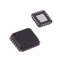
ADL5374ACPZ-R7 Analog Devices Inc, ADL5374ACPZ-R7 Datasheet - Page 12

ADL5374ACPZ-R7
Manufacturer Part Number
ADL5374ACPZ-R7
Description
IC MOD QUAD 3000-4000MHZ 24LFCSP
Manufacturer
Analog Devices Inc
Datasheet
1.ADL5374ACPZ-R7.pdf
(20 pages)
Specifications of ADL5374ACPZ-R7
Design Resources
Interfacing ADL5374 to AD9779A Dual-Channel, 1 GSPS High Speed DAC (CN0020)
Function
Modulator
Lo Frequency
2.8GHz ~ 4GHz
Rf Frequency
2.8GHz ~ 4GHz
P1db
12dBm
Noise Floor
-159.7dBm/Hz
Output Power
5dBm
Current - Supply
175mA
Voltage - Supply
4.75 V ~ 5.25 V
Test Frequency
3.8GHz
Package / Case
24-VFQFN, 24-CSP Exposed Pad
Frequency Range
3000MHz To 4000MHz
Rf Type
Quadrature
Supply Voltage Range
4.75V To 5.25V
Rf Ic Case Style
LFCSP
No. Of Pins
24
Operating Temperature Range
-40°C To +85°C
Lead Free Status / RoHS Status
Lead free / RoHS Compliant
Other names
ADL5374ACPZ-R7TR
ADL5374
BASIC CONNECTIONS
Figure 25 shows the basic connections for the ADL5374.
POWER SUPPLY AND GROUNDING
All the VPSx pins must be connected to the same 5 V source.
Adjacent pins of the same name can be tied together and decoupled
with a 0.1 μF capacitor. These capacitors should be located as
close as possible to the device. The power supply can range
between 4.75 V and 5.25 V.
The COM1 pin, COM2 pin, COM3 pin, and COM4 pin should
be tied to the same ground plane through low impedance paths.
COM1
COM1
VPS1
VPS1
VPS1
VPS1
C12
0.1µF
QBBP
1
2
3
4
5
6
GND
RLOP
OPEN
Figure 25. Basic Connections for the ADL5374
100pF
CLOP
NC
3600BL14M050
TECHNOLOGY
JOHANSON
EXPOSED PADDLE
4
5
6
QBBN
T1
F-MOD
Z1
CLON
100pF
3
2
1
IBBN
LO
RLON
OPEN
IBBP
18
17
16
15
14
13
100pF
COUT
VPS5
VPS4
VPS3
VPS2
VPS2
VOUT
0.1µF
C13
C16
0.1µF
C15
0.1µF
C14
0.1µF
OPEN
C11
VPOS
VOUT
Rev. 0 | Page 12 of 20
The exposed paddle on the underside of the package should also
be soldered to a low thermal and electrical impedance ground
plane. If the ground plane spans multiple layers on the circuit
board, they should be stitched together with nine vias under the
exposed paddle. The
thermal and electrical grounding of the LFCSP in detail.
BASEBAND INPUTS
The baseband inputs QBBP, QBBN, IBBP, and IBBN must be
driven from a differential source. The nominal drive level of
1.4 V p-p differential (700 mV p-p on each pin) should be
biased to a common-mode level of 500 mV dc.
The dc common-mode bias level for the baseband inputs may
range from 400 mV to 600 mV, which results in a reduction in
the usable input ac swing range. The nominal dc bias of 500 mV
allows for the largest ac swing, limited on the bottom end by the
ADL5374 input range and on the top end by the output compliance
range on most DACs from Analog Devices.
LO INPUT
The LO input should be driven differentially. The recommended
balun for the ADL5374 is the Johanson Technology model
3600BL14M050. The LO pins (LOIP and LOIN) should be ac-
coupled to the balun. A noticeable degradation in second-order
distortion and IP2 occurs when the device is driven single-ended.
The nominal LO drive of 0 dBm can be increased up to 6 dBm to
realize a slight improvement in the noise performance of the
modulator. If the LO source cannot provide the 0 dBm level,
operation at a reduced power below 0 dBm is acceptable.
Reduced LO drive results in slightly increased modulator noise.
The effect of LO power on sideband suppression and carrier
feedthrough is shown in Figure 20 and Figure 21.
RF OUTPUT
The RF output is available at the VOUT pin (Pin 13). The VOUT
pin connects to an internal balun, which is capable of driving a
50 Ω load. For applications requiring 50 Ω output impedance,
external matching is needed (see Figure 8 for S22 performance).
The internal balun provides a low dc path to ground. In most
situations, the VOUT pin should be ac-coupled to the load.
AN-772
application note discusses the


