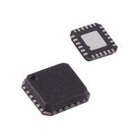
ADL5374ACPZ-R7 Analog Devices Inc, ADL5374ACPZ-R7 Datasheet - Page 13

ADL5374ACPZ-R7
Manufacturer Part Number
ADL5374ACPZ-R7
Description
IC MOD QUAD 3000-4000MHZ 24LFCSP
Manufacturer
Analog Devices Inc
Datasheet
1.ADL5374ACPZ-R7.pdf
(20 pages)
Specifications of ADL5374ACPZ-R7
Design Resources
Interfacing ADL5374 to AD9779A Dual-Channel, 1 GSPS High Speed DAC (CN0020)
Function
Modulator
Lo Frequency
2.8GHz ~ 4GHz
Rf Frequency
2.8GHz ~ 4GHz
P1db
12dBm
Noise Floor
-159.7dBm/Hz
Output Power
5dBm
Current - Supply
175mA
Voltage - Supply
4.75 V ~ 5.25 V
Test Frequency
3.8GHz
Package / Case
24-VFQFN, 24-CSP Exposed Pad
Frequency Range
3000MHz To 4000MHz
Rf Type
Quadrature
Supply Voltage Range
4.75V To 5.25V
Rf Ic Case Style
LFCSP
No. Of Pins
24
Operating Temperature Range
-40°C To +85°C
Lead Free Status / RoHS Status
Lead free / RoHS Compliant
Other names
ADL5374ACPZ-R7TR
OPTIMIZATION
The carrier feedthrough and sideband suppression performance of
the ADL5374 can be improved by using optimization techniques.
Carrier Feedthrough Nulling
Carrier feedthrough results from minute dc offsets that occur
between each of the differential baseband inputs. In an ideal
modulator, the quantities (V
equal to zero, which results in no carrier feedthrough. In a real
modulator, those two quantities are nonzero and, when mixed
with the LO, result in a finite amount of carrier feedthrough. The
ADL5374 is designed to provide a minimal amount of carrier
feedthrough. Should even lower carrier feedthrough levels be
required, minor adjustments can be made to the (V
and (V
while the Q-channel offset is varied until a minimum carrier
feedthrough level is obtained. The Q-channel offset required to
achieve this minimum is held constant, while the offset on the
I-channel is adjusted until a new minimum is reached. Through
two iterations of this process, the carrier feedthrough can be
reduced to as low as the output noise. The ability to null is
sometimes limited by the resolution of the offset adjustment.
Figure 26 shows the relationship of carrier feedthrough vs. dc
offset as null.
Note that throughout the nulling process, the dc bias for the
baseband inputs remains at 500 mV. When no offset is applied,
When an offset of +V
The same applies to the Q channel.
V
V
V
V
V
Figure 26. Carrier Feedthrough vs. DC Offset Voltage at 3500 MHz
IBBP
IBBP
IBBP
IBBN
IBBP
QBBP
–60
–64
–68
–72
–76
–80
–84
–88
–300 –240 –180 –120
= V
− V
= 500 mV + V
− V
= 500 mV − V
− V
IBBN
IBBN
IBBN
QBBN
= 500 mV, or
= V
= V
) offsets. The I-channel offset is held constant,
IOS
IOS
IOS
= 0 V
IOS
is applied to the I-channel inputs,
IOS
/2, and
/2, such that
V
P
IBBP
–60
– V
N
− V
OFFSET (µV)
0
IBBN
60
) and (V
120
QBBP
180
IBBP
− V
240
− V
QBBN
IBBN
300
) are
Rev. 0 | Page 13 of 20
)
It is often desirable to perform a one-time carrier null calibra-
tion. This is usually performed at a single frequency. Figure 27
shows how carrier feedthrough varies with LO frequency over a
range of ±50 MHz on either side of a null at 3500 MHz.
Sideband Suppression Optimization
Sideband suppression results from relative gain and relative
phase offsets between the I-channel and Q-channel and can
be suppressed through adjustments to those two parameters.
Figure 28 illustrates how sideband suppression is affected by
the gain and phase imbalances.
Figure 28 underlines the fact that adjusting only one parameter
improves the sideband suppression only to a point, unless the
other parameter is also adjusted. For example, if the amplitude
offset is 0.25 dB, improving the phase imbalance by better than
1° does not yield any improvement in the sideband suppression.
For optimum sideband suppression, an iterative adjustment
between phase and amplitude is required.
The sideband suppression nulling can be performed either
through adjusting the gain for each channel or through the
modification of the phase and gain of the digital data coming
from the digital signal processor.
Figure 28. Sideband Suppression vs. Quadrature Phase Error for
Figure 27. Carrier Feedthrough vs. f
–30
–35
–40
–45
–50
–55
–60
–65
–70
–75
–80
–10
–20
–30
–40
–50
–60
–70
–80
–90
3450 3460 3470 3480 3490 3500 3510 3520 3530 3540 3550
0
0.01
2.5dB
1.25dB
0.5dB
0.25dB
0.125dB
0.05dB
0.025dB
0.0125dB
0dB
Various Quadrature Amplitude Offsets
0.1
PHASE ERROR (Degrees)
LO FREQUENCY (MHz)
1
LO
After Nulling at 3500 MHz
10
ADL5374
100


