AD831APZ Analog Devices Inc, AD831APZ Datasheet - Page 18
AD831APZ
Manufacturer Part Number
AD831APZ
Description
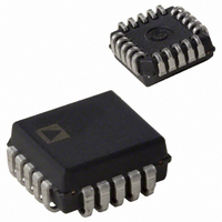
IC MIXER DWNCONV LOW DIST 20PLCC
Manufacturer
Analog Devices Inc
Series
AD831r
Specifications of AD831APZ
Rf Type
HF, VHF
Frequency
500MHz
Number Of Mixers
1
Gain
0dB
Noise Figure
14dB
Secondary Attributes
Down Converter
Current - Supply
125mA
Voltage - Supply
4.5 V ~ 5.5 V
Package / Case
20-LCC (J-Lead)
Supply Voltage Range
± 4.5V To ± 5.5V
Rf Ic Case Style
PLCC
No. Of Pins
20
Operating Temperature Range
-40°C To +85°C
Msl
MSL 1 - Unlimited
Termination Type
SMD
Operating Temperature (min)
-40C
Operating Temperature (max)
85C
Operating Temperature Classification
Industrial
Filter Terminals
SMD
Rohs Compliant
Yes
Lead Free Status / RoHS Status
Lead free / RoHS Compliant
Lead Free Status / RoHS Status
Lead free / RoHS Compliant, Lead free / RoHS Compliant
Available stocks
Company
Part Number
Manufacturer
Quantity
Price

Part Number:
AD831APZ
Manufacturer:
ADI/亚德诺
Quantity:
20 000
Company:
Part Number:
AD831APZ-REEL
Manufacturer:
PHI
Quantity:
2 000


ADL5350
2. Tune the LO port input network for optimum return
Table 8. Suggested RF, IF, and LO Filter Networks for Low-Side LO Injection
RF Frequency (MHz)
450
850
1950
2400
1
The inductor should have a self-resonant frequency greater than the intended frequency of operation. L1 should be a high Q inductor for optimum NF performance.
loss. Typically, a band-pass network is used to pass the
LO signal to the LOIN pin. It is recommended to block
high frequency harmonics of the LO from the mixer
core. LO harmonics cause higher RF frequency images
to be downconverted to the desired IF frequency and
result in sensitivity degradation. If the intended LO
source has poor harmonic distortion and spectral purity,
it may be necessary to employ a higher order band-pass
filter network. Figure 58 illustrates a simple LC band-
pass filter used to pass the fundamental frequency of the
LO source. Capacitor C3 is a simple dc block, while the
Series Inductor L3, along with the gate-to-source
capacitance of the buffer amplifier, form a low-pass
network. The native gate input of the LO buffer (FET)
alone presents a rather high input impedance. The gate
bias is generated internally using feedback that can result
in a positive return loss at the intended LO frequency.
L1 (nH)
8.3
6.8
1.7
0.67
1
C1 (pF)
10
4.7
1.5
1
Rev. 0 | Page 18 of 24
L2 (nH)
10
4.7
1.7
1.5
3. Design the RF and IF filter networks. Figure 58 depicts
If a better than −10 dB return loss is desired, it may be
necessary to add a shunt resistor to ground before the
coupling capacitor (C3) to present a lower loading
impedance to the LO source. In doing so, a slightly
greater LO drive level may be required.
simple LC tank filter networks for the IF and RF port
interfaces. The RF port LC network is designed to pass
the RF input signal. The series LC tank has a resonant
frequency at 1/(2π√LC). At resonance, the series reactances
are canceled, which presents a series short to the RF
signal. A parallel LC tank is used on the IF port to reject
the RF and LO signals. At resonance, the parallel LC tank
presents an open circuit.
It is necessary to account for the board parasitics, finite
Q, and self-resonant frequencies of the LC components
when designing the RF, IF, and LO filter networks. Table 8
provides suggested values for initial prototyping.
C2 (pF)
10
5.6
1.2
0.7
L3 (nH)
10
8.2
3.5
3.0
C3 (pF)
100
100
100
100
Related parts for AD831APZ
Image
Part Number
Description
Manufacturer
Datasheet
Request
R

Part Number:
Description:
MIXER IC
Manufacturer:
Analog Devices Inc
Datasheet:
Part Number:
Description:
MIXER IC
Manufacturer:
Analog Devices Inc
Datasheet:

Part Number:
Description:
±1.7g Dual-Axis IMEMS Accelerometer Evaluation Board
Manufacturer:
Analog Devices Inc
Datasheet:

Part Number:
Description:
Inertial Sensor Evaluation System
Manufacturer:
Analog Devices Inc
Datasheet:
Part Number:
Description:
Manufacturer:
Analog Devices Inc
Datasheet:
Part Number:
Description:
Manufacturer:
Analog Devices Inc
Datasheet:
Part Number:
Description:
Manufacturer:
Analog Devices Inc
Datasheet:
Part Number:
Description:
Manufacturer:
Analog Devices Inc
Datasheet:
Part Number:
Description:
Manufacturer:
Analog Devices Inc
Datasheet:
Part Number:
Description:
Manufacturer:
Analog Devices Inc
Datasheet:
Part Number:
Description:
Manufacturer:
Analog Devices Inc
Datasheet:
Part Number:
Description:
Manufacturer:
Analog Devices Inc
Datasheet: