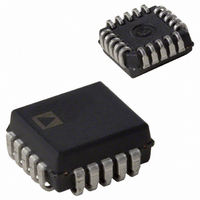
AD831APZ Analog Devices Inc, AD831APZ Datasheet

AD831APZ
Specifications of AD831APZ
Available stocks
Related parts for AD831APZ
AD831APZ Summary of contents
Page 1
FEATURES Broadband radio frequency (RF), intermediate frequency (IF), and local oscillator (LO) ports Conversion loss: 6.8 dB Noise figure: 6.5 dB High input IP3: 25 dBm High input P1dB: 19 dBm Low LO drive level Single-ended design: no need for ...
Page 2
ADL5350 TABLE OF CONTENTS Features .............................................................................................. 1 Applications....................................................................................... 1 Functional Block Diagram .............................................................. 1 General Description ......................................................................... 1 Revision History ............................................................................... 2 Specifications..................................................................................... 3 850 MHz Receive Performance .................................................. 3 1950 MHz Receive Performance ................................................ 3 Spur Tables......................................................................................... 4 850 ...
Page 3
SPECIFICATIONS 850 MHz RECEIVE PERFORMANCE 25°C, LO power = 4 dBm, re: 50 Ω, unless otherwise noted Table 1. Parameter RF Frequency Range LO Frequency Range IF Frequency Range Conversion Loss SSB ...
Page 4
ADL5350 SPUR TABLES All spur tables are (N × − (M × mixer spurious products for 0 dBm input power, unless otherwise noted. N.M. indicates that spur was not measured due to it ...
Page 5
ABSOLUTE MAXIMUM RATINGS Table 5. Parameter Supply Voltage Input Level LO Input Level Internal Power Dissipation θ JA Maximum Junction Temperature Operating Temperature Range Storage Temperature Range Stresses above those listed under Absolute Maximum Ratings Rating may ...
Page 6
ADL5350 PIN CONFIGURATION AND FUNCTION DESCRIPTIONS Table 6. Pin Function Descriptions Pin No. Mnemonic Description 1, 8 RF/IF RF and IF Input/Output Ports. These nodes are internally tied together. RF and IF port separation is achieved using external tuning networks. ...
Page 7
TYPICAL PERFORMANCE CHARACTERISTICS 850 MHz CHARACTERISTICS Supply voltage = frequency = 850 MHz, IF frequency = 70 MHz, RF level = 0 dBm, LO level = 4 dBm ...
Page 8
Supply voltage = frequency = 850 MHz, IF frequency = 70 MHz, RF level = 0 dBm, LO level = 4 dBm +85° 2.7 2.8 2.9 3.0 3.1 3.2 ...
Page 9
Supply voltage = frequency = 850 MHz, IF frequency = 70 MHz, RF level = 0 dBm, LO level = 4 dBm –40°C 20 +25°C 19 +85° 750 775 800 ...
Page 10
ADL5350 Supply voltage = frequency = 850 MHz, IF frequency = 70 MHz, RF level = 0 dBm, LO level = 4 dBm 100 ...
Page 11
Supply voltage = frequency = 850 MHz, IF frequency = 70 MHz, RF level = 0 dBm, LO level = 4 dBm, T –13 –14 –15 –16 –17 –40°C –18 +25°C –19 –20 +85°C –21 750 775 ...
Page 12
ADL5350 1950 MHz CHARACTERISTICS Supply voltage = frequency = 1950 MHz, IF frequency = 190 MHz, RF level = −10 dBm, LO level = 6 dBm, T unless otherwise noted ...
Page 13
Supply voltage = frequency = 1950 MHz, IF frequency = 190 MHz, RF level = −10 dBm, LO level = 6 dBm, T unless otherwise noted +85°C 26 +25°C 25 –40° 2.7 ...
Page 14
ADL5350 Supply voltage = frequency = 1950 MHz, IF frequency = 190 MHz, RF level = −10 dBm, LO level = 6 dBm, T unless otherwise noted –40°C 20 +25° +85°C 17 ...
Page 15
Supply voltage = frequency = 1950 MHz, IF frequency = 190 MHz, RF level = −10 dBm, LO level = 6 dBm, T unless otherwise noted 100 150 200 ...
Page 16
ADL5350 Supply voltage = frequency = 1950 MHz, IF frequency = 190 MHz, RF level = −10 dBm, LO level = 6 dBm, T unless otherwise noted. –8 –9 –10 –11 –12 –13 –14 –15 1800 1825 ...
Page 17
FUNCTIONAL DESCRIPTION CIRCUIT DESCRIPTION The ADL5350 is a GaAs pHEMT, single-ended, passive mixer with an integrated LO buffer amplifier. The device relies on the varying drain to source channel conductance of a FET junction to modulate an RF signal. A ...
Page 18
ADL5350 2. Tune the LO port input network for optimum return loss. Typically, a band-pass network is used to pass the LO signal to the LOIN pin recommended to block high frequency harmonics of the LO from the ...
Page 19
APPLICATIONS INFORMATION LOW FREQUENCY APPLICATIONS The ADL5350 can be used in low frequency applications. The circuit in Figure 59 is designed for 136 MHz to 176 MHz and MHz using a high-side LO. ...
Page 20
ADL5350 Figure 63 depicts a crossover filter network approach to provide isolation between the RF and IF ports for a downconverting application. The crossover network essentially provides a high- pass filter to allow the RF signal to pass to the ...
Page 21
EVALUATION BOARD An evaluation board is available for the ADL5350. The evaluation board has two halves: a low band board designated as Board A and a high band board designated as Board B. The schematic for the evaluation board is ...
Page 22
ADL5350 OUTLINE DIMENSIONS PIN 1 INDICATOR 1.00 0.85 0.80 SEATING ORDERING GUIDE Model Temperature Range 1 ADL5350ACPZ-R7 −40°C to +85°C 1 ADL5350ACPZ-WP −40°C to +85°C 1 ADL5350-EVALZ RoHS Compliant Part. 3.25 3.00 2.75 0.60 0.45 2.25 1.95 ...
Page 23
NOTES Rev Page ADL5350 ...
Page 24
ADL5350 NOTES ©2008 Analog Devices, Inc. All rights reserved. Trademarks and registered trademarks are the property of their respective owners. D05615-0-2/08(0) Rev Page ...


