AD831APZ Analog Devices Inc, AD831APZ Datasheet - Page 17
AD831APZ
Manufacturer Part Number
AD831APZ
Description
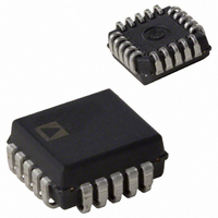
IC MIXER DWNCONV LOW DIST 20PLCC
Manufacturer
Analog Devices Inc
Series
AD831r
Specifications of AD831APZ
Rf Type
HF, VHF
Frequency
500MHz
Number Of Mixers
1
Gain
0dB
Noise Figure
14dB
Secondary Attributes
Down Converter
Current - Supply
125mA
Voltage - Supply
4.5 V ~ 5.5 V
Package / Case
20-LCC (J-Lead)
Supply Voltage Range
± 4.5V To ± 5.5V
Rf Ic Case Style
PLCC
No. Of Pins
20
Operating Temperature Range
-40°C To +85°C
Msl
MSL 1 - Unlimited
Termination Type
SMD
Operating Temperature (min)
-40C
Operating Temperature (max)
85C
Operating Temperature Classification
Industrial
Filter Terminals
SMD
Rohs Compliant
Yes
Lead Free Status / RoHS Status
Lead free / RoHS Compliant
Lead Free Status / RoHS Status
Lead free / RoHS Compliant, Lead free / RoHS Compliant
Available stocks
Company
Part Number
Manufacturer
Quantity
Price

Part Number:
AD831APZ
Manufacturer:
ADI/亚德诺
Quantity:
20 000
Company:
Part Number:
AD831APZ-REEL
Manufacturer:
PHI
Quantity:
2 000


INPUT
FUNCTIONAL DESCRIPTION
CIRCUIT DESCRIPTION
The ADL5350 is a GaAs pHEMT, single-ended, passive
mixer with an integrated LO buffer amplifier. The device
relies on the varying drain to source channel conductance
of a FET junction to modulate an RF signal. A simplified
schematic is shown in Figure 57.
The LO signal is applied to the gate contact of a FET-based
buffer amplifier. The buffer amplifier provides sufficient
gain of the LO signal to drive the resistive switch. Additionally,
feedback circuitry provides the necessary bias to the FET
buffer amplifier and RF/IF ports to achieve optimum
modulation efficiency for common cellular frequencies.
The mixing of RF and LO signals is achieved by switching
the channel conductance from the RF/IF port to ground at
the rate of the LO. The RF signal is passed through an external
band-pass network to help reject image bands and reduce
the broadband noise presented to the mixer. The band-
limited RF signal is presented to the time-varying load of
the RF/IF port, which causes the envelope of the RF signal
to be amplitude modulated at the rate of the LO. A filter
network applied to the IF port is necessary to reject the
RF signal and pass the wanted mixing product. In a down-
conversion application, the IF filter network is designed to
pass the difference frequency and present an open circuit
to the incident RF frequency. Similarly, for an upconversion
application, the filter is designed to pass the sum frequency
and reject the incident RF. As a result, the frequency response
of the mixer is determined by the response characteristics
of the external RF/IF filter networks.
LO
LOIN
VPOS
Figure 57. Simplified Schematic
V
S
GND1
OR OUTPUT
INPUT
RF
GND2
RF
IF
IF
OUTPUT
OR INPUT
Rev. 0 | Page 17 of 24
IMPLEMENTATION PROCEDURE
The ADL5350 is a simple single-ended mixer that relies
on off-chip circuitry to achieve effective RF dynamic
performance. The following steps should be followed
to achieve optimum performance (see Figure 58 for
component designations):
1. Table 7 shows the recommended LO bias inductor
Table 7. Recommended LO Bias Inductor
Desired LO Frequency (MHz)
380
750
1000
1750
2000
1
the intended frequency of operation.
The bias inductor should have a self-resonant frequency greater than
values for a variety of LO frequencies. To ensure efficient
commutation of the mixer, the bias inductor needs to
be properly set. For other frequencies within the range
shown, the values can be interpolated. For frequencies
outside this range, see the Applications Information section.
RF
IF
Figure 58. Reference Schematic
L1
L2
C1
RF/IF
RF/IF
8
1
C6
C2
GND2
NC
ADL5350
7
2
Recommended LO Bias
Inductor, L4
68
24
18
3.8
2.1
VPOS
LOIN
LO
V
6
3
S
L4
L3
C3
C4
GND1
NC
5
4
1
ADL5350
(nH)
Related parts for AD831APZ
Image
Part Number
Description
Manufacturer
Datasheet
Request
R

Part Number:
Description:
MIXER IC
Manufacturer:
Analog Devices Inc
Datasheet:
Part Number:
Description:
MIXER IC
Manufacturer:
Analog Devices Inc
Datasheet:

Part Number:
Description:
±1.7g Dual-Axis IMEMS Accelerometer Evaluation Board
Manufacturer:
Analog Devices Inc
Datasheet:

Part Number:
Description:
Inertial Sensor Evaluation System
Manufacturer:
Analog Devices Inc
Datasheet:
Part Number:
Description:
Manufacturer:
Analog Devices Inc
Datasheet:
Part Number:
Description:
Manufacturer:
Analog Devices Inc
Datasheet:
Part Number:
Description:
Manufacturer:
Analog Devices Inc
Datasheet:
Part Number:
Description:
Manufacturer:
Analog Devices Inc
Datasheet:
Part Number:
Description:
Manufacturer:
Analog Devices Inc
Datasheet:
Part Number:
Description:
Manufacturer:
Analog Devices Inc
Datasheet:
Part Number:
Description:
Manufacturer:
Analog Devices Inc
Datasheet:
Part Number:
Description:
Manufacturer:
Analog Devices Inc
Datasheet: