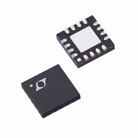
LTC4557EUD Linear Technology, LTC4557EUD Datasheet - Page 8

LTC4557EUD
Manufacturer Part Number
LTC4557EUD
Description
IC DUAL SIM/SMART CARD PS 16QFN
Manufacturer
Linear Technology
Datasheet
1.LTC4557EUD.pdf
(12 pages)
Specifications of LTC4557EUD
Function
Power Management, Signal Level Translation
Rf Type
Cellular, 3G, GSM
Secondary Attributes
SIM & Smart Card Interface
Package / Case
16-WFQFN Exposed Pad
Lead Free Status / RoHS Status
Contains lead / RoHS non-compliant
Available stocks
Company
Part Number
Manufacturer
Quantity
Price
Company:
Part Number:
LTC4557EUD
Manufacturer:
LT
Quantity:
10 000
Part Number:
LTC4557EUD
Manufacturer:
LINEAR
Quantity:
20 000
OPERATIO
LTC4557
Activation/Deactivation
Activation and deactivation sequencing is handled by
built-in circuitry. The activation sequence is initiated by
bringing the ENABLE pin HIGH. The activation sequence is
outlined below:
1. The RST, CLK and I/O pins are held LOW.
2. V
3. After V
4. The clock channel is enabled on the rising edge of the
The deactivation sequence is initiated by bringing the
ENABLE pin LOW. The deactivation sequence is outlined
below:
1. The reset channel is disabled and RST is brought LOW.
2. The clock channel is disabled and the CLK pin is brought
8
channels are enabled.
second clock cycle after the I/O pin is enabled.
LOW two clock cycles after ENABLE is brought LOW. If
the clock is not running, the clock channel will be
disabled approximately 9 s after the ENABLE pin is
brought LOW.
CC
is enabled.
CC
is stable at its selected level, The I/O and RST
U
3. The I/O channel is disabled and the I/O pin is brought
4. V
The activation or deactivation sequences will take place
every time a card socket is enabled or disabled.
Fault Protection
The V
short-circuit faults. While there are no logic outputs to
indicate that a fault has occurred, these pins will be able
to tolerate the fault condition until it has been removed.
The V
tion circuitry which will limit the current available to the
pins. Each V
90mA (typ) before the output voltage is reduced.
The CLKA,B pins are designed to tolerate faults by reduc-
ing the current drive capability of their output stages. After
a fault is detected by the internal fault detection logic, the
logic waits for a fault detection delay to elapse before
reducing the current drive capability of the output stage.
LOW approximately 9 s after the ENABLE is brought
LOW.
CC
CCA,B
CC
will be depowered after the I/O pin is brought LOW.
, I/O, RST and CLK pins are all protected against
, I/OA,B, and RSTA,B pins possess fault protec-
CC
pin is capable of supplying approximately
4557f


