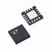
LTC4557EUD Linear Technology, LTC4557EUD Datasheet - Page 5

LTC4557EUD
Manufacturer Part Number
LTC4557EUD
Description
IC DUAL SIM/SMART CARD PS 16QFN
Manufacturer
Linear Technology
Datasheet
1.LTC4557EUD.pdf
(12 pages)
Specifications of LTC4557EUD
Function
Power Management, Signal Level Translation
Rf Type
Cellular, 3G, GSM
Secondary Attributes
SIM & Smart Card Interface
Package / Case
16-WFQFN Exposed Pad
Lead Free Status / RoHS Status
Contains lead / RoHS non-compliant
Available stocks
Company
Part Number
Manufacturer
Quantity
Price
Company:
Part Number:
LTC4557EUD
Manufacturer:
LT
Quantity:
10 000
Part Number:
LTC4557EUD
Manufacturer:
LINEAR
Quantity:
20 000
PI FU CTIO S
DV
logic.
V
sections of the LTC4557.
V
should be connected to the V
sockets. The activation of the V
by the M0, M1 and ENABLE inputs. They can be set to 0V,
1.8V or 3V. Only one of the two, either V
be active at a time.
CLKA/CLKB (Pins 5, 16): Card Socket. The CLKA/CLKB
pins should be connected to the CLK pins of the respective
card sockets. The CLKA/CLKB signals are derived from the
CLKIN pin. They provide a level shifted CLKIN signal to the
selected card. The CLKA/CLKB pins are gated off until
V
RSTA/RSTB (Pins 6, 15): Card Socket. The RSTA/RSTB
pins should be connected to the RST pins of the respective
card sockets. The RSTA/RSTB signals are derived from
the RSTIN pin. When a card is selected, its RST pin follows
RSTIN. The RSTA/RSTB pins are gated off until V
attain their correct values.
I/OA, I/OB (Pins 7, 14): Card Socket. The I/OA, I/OB pins
connect to the I/O pins of the respective card sockets.
When a card is selected, its I/O pin transmits/receives data
to/from the DATA pin. The I/OA, I/OB pins are gated off
until V
BATT
CCA
CCA
U
CC
/V
/V
(Pin 2): Power. Reference voltage for the control
CCA
(Pin 3): Power. Supply voltage for the analog
CCB
CCB
/V
U
(Pins 4, 1): Card Socket. The V
attain their correct values.
CCB
attain their correct values.
U
CC
CCA
pins of the respective card
/V
CCB
pins is controlled
CCA
CCA
or V
/V
CCA
CCB
CCB
/V
, may
pins
CCB
DATA (Pin 8): Input/Output. Microcontroller side data I/O
pin. The DATA pin provides the bidirectional communica-
tion path to both cards. Only one of the cards may be
selected to communicate via the DATA pin. The pin pos-
sesses a dynamically activated pull-up current source,
allowing the controller to use an open-drain output. The
current source maintains a HIGH state. This pin is held
HIGH by a weak pull-up when the ENABLE pin is LOW.
RSTIN (Pin 9): Input. The RSTIN pin supplies the reset
signal to the cards. It is level shifted and transmitted
directly to the RST pin of the selected card.
CLKIN (Pin 10): Input. The CLKIN pin supplies the clock
signal to the cards. It is level shifted and transmitted
directly to the CLK pin of the selected card.
M0/M1 (Pins 12, 11): Inputs. The M0 and M1 pins select
which set of SIM/smart card pins are active and at which
voltage level they operate. The truth table for these pins
follows:
ENABLE (Pin 13): Input. The ENABLE pin shuts down the
chip when LOW.
EXPOSED PAD (Pin 17): Chip Ground. This ground pad
must be soldered directly to a PCB ground plane.
M1
0
0
1
1
M0
0
1
0
1
SELECTED CARD/VOLTAGE
Card A/1.8V
Card A/3V
Card B/1.8V
Card B/3V
LTC4557
5
4557f


