EVAL-869-ES Linx Technologies Inc, EVAL-869-ES Datasheet - Page 2
EVAL-869-ES
Manufacturer Part Number
EVAL-869-ES
Description
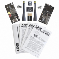
KIT EVAL BASIC 869MHZ ES SERIES
Manufacturer
Linx Technologies Inc
Series
ESr
Type
Transmitter, Receiverr
Specifications of EVAL-869-ES
Frequency
869MHz
Product
RF Development Tools
Maximum Frequency
868 MHz
Supply Voltage (max)
5 V
Lead Free Status / RoHS Status
Lead free / RoHS Compliant
For Use With/related Products
Linx OEM Module
Lead Free Status / Rohs Status
Lead free / RoHS Compliant


Table 1: ES Series Transmitter Specifications
Notes
1. Center frequency measured while modulated with a 0-5V square wave.
2. Into a 50-ohm load.
3. LADJ open.
4. Maximum power when LADJ open, minimum power when LADJ grounded.
5. DATA pin modulated with a 0-5V square wave.
6. The audio bandwidth is wide to accommodate the needs of the data slicer.
7. Characterized, but not tested.
8. The ES is optimized for both 0-5V and 0-3V modulation when sending digital data.
9. Analog signals, including audio, should be AC-coupled.
10. Time to transmitter readiness from the application of power to V
11. Maximum time without a data transition.
Page 2
ELECTRICAL SPECIFICATIONS
Parameter
POWER SUPPLY
Operating Voltage
Supply Current
Power-Down Current
TRANSMIT SECTION
Transmit Frequency:
Center Frequency Accuracy
Output Power
Output Power Control Range
Harmonic Emissions
Frequency Deviation
Data Rate
Analog/Audio Bandwidth
Data Input:
Power-Down Input:
Analog Input
ANTENNA PORT
RF Output Impedance
TIMING
Transmitter Turn-On Time
Max. Time Between Transitions
ENVIRONMENTAL
Operating Temperature Range
TXM-916-ES
TXM-869-ES
TXM-916-ES
TXM-869-ES
Logic Low
Logic High
Logic Low
Logic High
*CAUTION*
This product incorporates numerous static-sensitive components.
Always wear an ESD wrist strap and observe proper ESD handling
procedures when working with this device. Failure to observe this
precaution may result in module damage or failure.
Designation
R
F
V
I
I
PDN
P
P
V
V
F
CC
DEV
OUT
–
–
–
–
–
–
–
–
–
–
–
–
CC
IH
C
O
H
IL
Min.
200
2.1
5.5
-60
0.0
3.0
0.0
1.5
0.0
0.1
-3
80
70
20
–
–
–
–
–
–
–
0
Typical
916.48
869.85
90.0
3.0
7.0
-55
0.5
CC
65
50
–
0
–
–
–
–
–
–
–
–
–
–
–
or PDN going high.
56,000
28,000
Max.
+60
130
130
V
+70
4.0
8.5
-47
0.4
5.2
0.7
5.0
1.5
5.0
+4
–
–
–
–
–
CC
Units
mSec
mSec
VDC
MHz
MHz
dBm
VDC
VDC
VDC
VDC
kHz
dBc
kHz
kHz
V
mA
bps
µA
dB
Hz
°
Ω
P-P
C
Notes
2,3,7
7,10
7,11
2,3
6,7
–
–
7
4
4
1
2
5
5
7
8
8
–
–
9
7
7
Figure 3: Level Adjust Attenuation
Figure 5: Tx Powerup to Valid Rx Analog
ABSOLUTE MAXIMUM RATINGS
PERFORMANCE DATA
TYPICAL PERFORMANCE GRAPHS
1
2
CH1 2.00V
40
35
30
25
20
15
-10
These performance parameters are
based on module operation at 25°C
from a 3.0VDC supply unless
otherwise noted. Figure 2 illustrates
the connections necessary for
testing
recommended all ground pins be
connected to the ground plane.
-8.0
Supply voltage V
Any Input or Output Pin
Operating Temperature
Storage Temperature
Soldering Temperature
*NOTE*
damage to the device. Furthermore, extended operation at these maximum
ratings may reduce the life of this device.
CH2 500mV
Tx VCC/PDN
Rx Demodulated Analog Data
RF Output Attenuation (dB)
-6.0
and
-4.0
Exceeding any of the limits of this section may lead to permanent
100uS
operation.
-2.0
CC
-1.0
-0.4
It
-0.2
is
Figure 2: Test / Basic Application Circuit
Figure 4: Square-Wave Modulation Linearity
Figure 6: Tx Powerup to Valid Rx Data
1
2
1
2
-0.3
-0.5
-40
CH1 2.00V
CH1 1.66V
0
+216°C for 15 seconds
OUT
IN
RX Data
Tx VCC/PDN
1
2
3
4
5
CH2 2.00V
CH2 100mV
to
to V
to
to
PDN
LADJ
VCC
GND
DATA
CC
1mS
+4.0
+70
+90
LO_V_D
/CLK SE
250uS
+ 0.5
GND
/CLK
ANT
VDC
VDC
°C
°C
10
9
8
7
6
Page 3
Related parts for EVAL-869-ES
Image
Part Number
Description
Manufacturer
Datasheet
Request
R

Part Number:
Description:
ENERCHIP CC EVAL KIT
Manufacturer:
Cymbet Corporation
Datasheet:

Part Number:
Description:
BOARD EVAL FOR AD976
Manufacturer:
Analog Devices Inc
Datasheet:

Part Number:
Description:
BOARD EVAL FOR ADXL345
Manufacturer:
Analog Devices Inc
Datasheet:

Part Number:
Description:
ENERCHIP CC SEH EVAL KIT
Manufacturer:
Cymbet Corporation
Datasheet:

Part Number:
Description:
ENERCHIP EP ENERGY HARVEST EVAL
Manufacturer:
Cymbet Corporation
Datasheet:

Part Number:
Description:
EVAL BOARD FOR TW6864-LB2-GR
Manufacturer:
Intersil
Datasheet:
Part Number:
Description:
EVAL BOARD FOR TW8816-LB3-GR
Manufacturer:
Intersil
Datasheet:
Part Number:
Description:
EVAL BOARD FOR TW8817-TA3-GRS
Manufacturer:
Intersil
Datasheet:

Part Number:
Description:
EVALUATION MODULE FOR ADUM4160
Manufacturer:
Analog Devices Inc
Datasheet:

Part Number:
Description:
BOARD EVALUATION ADCMP581BCP
Manufacturer:
Analog Devices Inc
Datasheet:
Part Number:
Description:
BOARD EVALUATION ADM1041
Manufacturer:
Analog Devices Inc
Datasheet:

Part Number:
Description:
EVAL BOARD FOR STM32F107VCT
Manufacturer:
STMicroelectronics
Datasheet:
Part Number:
Description:
BOARD EVAL FOR AD1954
Manufacturer:
Analog Devices Inc
Datasheet:
Part Number:
Description:
BOARD EVAL FOR AD1955
Manufacturer:
Analog Devices Inc
Datasheet:

Part Number:
Description:
BOARD EVAL FOR AD7655
Manufacturer:
Analog Devices Inc
Datasheet: