RF3854PCK-410 RFMD, RF3854PCK-410 Datasheet - Page 4
RF3854PCK-410
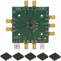
Manufacturer Part Number
RF3854PCK-410
Description
KIT EVAL FOR RF3854
Manufacturer
RFMD
Type
Modulator, PA Driverr
Datasheet
1.RF3854PCK-410.pdf
(26 pages)
Specifications of RF3854PCK-410
Frequency
800MHz ~ 2GHz
For Use With/related Products
RF3854
Lead Free Status / RoHS Status
Lead free / RoHS Compliant
Other names
689-1053
RF3854PCBA
RF3854PCBA


RF3854
4 of 26
General Conditions
Local Oscillator
IQ Baseband Inputs
Output Performance with Modulated Baseband Inputs
W-CDMA Mode
Mode=Wideband F
Settings)
Output Power
Maximum Output Power with
Gain Range
Gain Step
Out-of-Band Emission
Adjacent Channel Leakage Power
Channel Spacing
Error Vector Magnitude
RMS*
Output Noise
At F
* Not tested in Production
High Power to Medium Power
W-CDMA Modulated Signal*
Ratio (ALCR)*
C
Medium Power to Low Power
±40MHz*
Baseband Filter Attenuation
RF HB Output Frequency
LO HB Input Frequency
Parameter
Medium Power Mode
IQ Common Mode
High Power Mode
High Power Mode
Input Bandwidth
Input Power
LO
±10MHz
IQ Level
±5MHz
x2 (see Control Logic Truth Table for Mode Control
7628 Thorndike Road, Greensboro, NC 27409-9421 · For sales or technical
support, contact RFMD at (+1) 336-678-5570 or sales-support@rfmd.com.
Min.
1710
1710
-6.0
0.7
20
-4
3
Specification
Typ.
±0.5
-152
TBD
0.0
1.4
1.2
1.2
1.0
90
50
65
-1
6
Max.
1910
1910
+3.0
-146
-146
dBc/Hz
dBc/Hz
%rms
Unit
dBm
dBm
dBm
MHz
MHz
MHz
V
dBc
dBc
dB
dB
dB
dB
P-P
V
8PSK
Input IQ signal driven differentially and in
quadrature.
At 20MHz offset
V
ALCR
GC=2.0V
GC=1.5V
Difference between output power at GC=2.0V
and GC=0.2V.
Gain step when switching between power
modes in either direction.
GC=1.4V
GC=TBD
3.84MHz relative to channel power
3.84MHz relative to channel power
3GPP W-CDMA
GC=2.0V
GC=2.0V to 1.5V
CC
=2.7V, T=+25°C, while meeting 48dBc
Condition
Rev A1 DS070313
Related parts for RF3854PCK-410
Image
Part Number
Description
Manufacturer
Datasheet
Request
R

Part Number:
Description:
IC AMP HBT GAAS CATV 8-SOIC
Manufacturer:
RFMD
Datasheet:

Part Number:
Description:
IC AMP MMIC GAAS 12GHZ 4-MICROX
Manufacturer:
RFMD
Datasheet:

Part Number:
Description:
IC AMP 3V LOW-NOISE SOT23-6
Manufacturer:
RFMD
Datasheet:

Part Number:
Description:
KIT EVAL FOR NBB-310
Manufacturer:
RFMD
Datasheet:
Part Number:
Description:
IC AMPLIFIER MMIC LNA 8-QFN
Manufacturer:
RFMD
Datasheet:
Part Number:
Description:
IC AMP MMIC GAAS 4GHZ 4-MICROX
Manufacturer:
RFMD
Datasheet:
Part Number:
Description:
IC SWITCH 10W PHEMT SPDT 12QFN
Manufacturer:
RFMD
Datasheet:
Part Number:
Description:
IC QUADRATURE MODULATOR 16-SOIC
Manufacturer:
RFMD
Datasheet:
Part Number:
Description:
100MHZ TO 4000MHZ, GAAS PHEMT MMIC LOW NOISE AMPLIFIERS
Manufacturer:
RFMD
Part Number:
Description:
KIT EVAL FOR RF2336
Manufacturer:
RFMD
Datasheet:


Part Number:
Description:
IC AMP WLAN/LNA DVR 3V SOT23-5
Manufacturer:
RFMD
Datasheet:

Part Number:
Description:
IC AMP HBT GAAS LNA BYPASS 8-QFN
Manufacturer:
RFMD
Datasheet:

Part Number:
Description:
IC AMP MMIC GAAS 10GHZ 4-MICROX
Manufacturer:
RFMD
Datasheet: