RF3854PCK-410 RFMD, RF3854PCK-410 Datasheet - Page 15
RF3854PCK-410
Manufacturer Part Number
RF3854PCK-410
Description
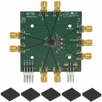
KIT EVAL FOR RF3854
Manufacturer
RFMD
Type
Modulator, PA Driverr
Datasheet
1.RF3854PCK-410.pdf
(26 pages)
Specifications of RF3854PCK-410
Frequency
800MHz ~ 2GHz
For Use With/related Products
RF3854
Lead Free Status / RoHS Status
Lead free / RoHS Compliant
Other names
689-1053
RF3854PCBA
RF3854PCBA


Rev A1 DS070313
Pin
12
13
14
15
16
17
18
19
Function
RF OUT
RF OUT
RF OUT
RF OUT
RF OUT
RF OUT
WB N
WB P
HB N
HB P
LB N
LB P
GND
GC
Description
Gain control voltage. Maximum output power at 2.0V. Minimum output
power at 0V. When the chip is enabled the input impedance is 10kΩ to
1.67V
input goes high impedance.
Differential low band PA driver amplifier output.
This output is intended for low band (GSM850/900) operation and drives a
differential SAW.
A bypass mode allows the low band PA driver amplifier’s input to be
switched between the signal from the modulator and the signal applied at
LOLB. This enables a GMSK-modulated signal on the LOLB input to be
switched into the RF signal path.
The output is an open collector. The outputs are matched off-chip.
Complementary differential low band PA driver amplifier output.
See pin 13.
Differential high band PA Driver amplifier output.
This output is intended for DCS1800/PCS1900 band operation.
A bypass mode allows the high band PA driver amplifier’s input to be
switched between the signal from the modulator and the signal applied at
LOHB. This enables a GMSK-modulated DCS1800/PCS1900 signal on the
LOHB input to be switched into the RF signal path.
The output is an open collector. The outputs are matched off-chip.
Complementary differential high band PA driver amplifier output.
See pin 15.
Differential high band PA driver amplifier output.
This output is intended for wide band (W-CDMA) applications.
The output is an open collector. The output are matched off-chip.
Complementary differential wideband PA driver amplifier output.
See pin 17.
Ground.
7628 Thorndike Road, Greensboro, NC 27409-9421 · For sales or technical
support, contact RFMD at (+1) 336-678-5570 or sales-support@rfmd.com.
DC
. When the chip is powered down a FET switch is opened and the
Interface Schematic
See pin 13.
See pin 15.
See pin 17.
V
CC2
10 k Ω
V
V
V
CC
CC
CC
RF3854
1.7 V
V
V
V
CC
CC
CC
-
+
V
V
4 k Ω
V
CC
CC
CC
RF OUT WB P
RF OUT WB N
RF OUT HB P
RF OUT HB N
15 of 26
RF OUT LB P
RF OUT LB N
Related parts for RF3854PCK-410
Image
Part Number
Description
Manufacturer
Datasheet
Request
R

Part Number:
Description:
IC AMP HBT GAAS CATV 8-SOIC
Manufacturer:
RFMD
Datasheet:

Part Number:
Description:
IC AMP MMIC GAAS 12GHZ 4-MICROX
Manufacturer:
RFMD
Datasheet:

Part Number:
Description:
IC AMP 3V LOW-NOISE SOT23-6
Manufacturer:
RFMD
Datasheet:

Part Number:
Description:
KIT EVAL FOR NBB-310
Manufacturer:
RFMD
Datasheet:
Part Number:
Description:
IC AMPLIFIER MMIC LNA 8-QFN
Manufacturer:
RFMD
Datasheet:
Part Number:
Description:
IC AMP MMIC GAAS 4GHZ 4-MICROX
Manufacturer:
RFMD
Datasheet:
Part Number:
Description:
IC SWITCH 10W PHEMT SPDT 12QFN
Manufacturer:
RFMD
Datasheet:
Part Number:
Description:
IC QUADRATURE MODULATOR 16-SOIC
Manufacturer:
RFMD
Datasheet:
Part Number:
Description:
100MHZ TO 4000MHZ, GAAS PHEMT MMIC LOW NOISE AMPLIFIERS
Manufacturer:
RFMD
Part Number:
Description:
KIT EVAL FOR RF2336
Manufacturer:
RFMD
Datasheet:


Part Number:
Description:
IC AMP WLAN/LNA DVR 3V SOT23-5
Manufacturer:
RFMD
Datasheet:

Part Number:
Description:
IC AMP HBT GAAS LNA BYPASS 8-QFN
Manufacturer:
RFMD
Datasheet:

Part Number:
Description:
IC AMP MMIC GAAS 10GHZ 4-MICROX
Manufacturer:
RFMD
Datasheet: