RF3854PCK-410 RFMD, RF3854PCK-410 Datasheet - Page 19
RF3854PCK-410
Manufacturer Part Number
RF3854PCK-410
Description
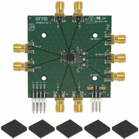
KIT EVAL FOR RF3854
Manufacturer
RFMD
Type
Modulator, PA Driverr
Datasheet
1.RF3854PCK-410.pdf
(26 pages)
Specifications of RF3854PCK-410
Frequency
800MHz ~ 2GHz
For Use With/related Products
RF3854
Lead Free Status / RoHS Status
Lead free / RoHS Compliant
Other names
689-1053
RF3854PCBA
RF3854PCBA


The baseband inputs of the RF3854 must be driven with balanced signals. Amplitude and phase matching <0.5dB and <0.5
degrees are recommended. Phase or gain imbalances between the complementary input signals will cause additional distor-
tion including some second order baseband distortion.
The RF3854 is designed to be driven with either single-ended or differential LO signals. Driving the chip differentially is benefi-
cial in improving the LO leakage performance. Decreasing the LO drive level will also improve LO leakage, but the output noise
performance will be degraded. Driving the LO level too high will degrade linearity.
The ground lines for the LO sections are brought out of the chip independently from the ground to the RF and modulator sec-
tions. This is intended to give the board design the independence of isolating the LO signals from the RF output sections.
The RF3854 includes frequency doubler and divider modes that allow the LO to operate at half or twice the frequency depend-
ing on the application. This provides some flexibility in improving VCO isolation and LO leakage through frequency translation.
The RF outputs use open collector architecture and may be biased at voltages higher than V
voltage may improve the intermodulation performance. The load resistors are selected to provide sufficient output power while
maintaining good linearity.
The GC DEC and V
are recommended. The purpose of these capacitors is to filter out low frequency noise (20MHz) in the gain control lines that
may cause noise on the RF signal. The capacitor on the GC DEC line will effect the settling time of the step response in power
control voltage. A 1nF capacitor equates to around a 200ns settling time; a 0.5nF capacitor equates to a 100ns settling time.
There is a trade-off between setting time and phase noise as gain control is applied.
As with any RF circuit, the RF3854 is sensitive to PC board layout. The suggested schematic and board layout is included as a
guideline. Proper grounding of the die flag under the chip is essential in achieving acceptable RF performance. A symmetric
output structure will maintain signal balance while keeping the RF lines short will reduce losses. Proper routing and bypassing
of the supply lines will improve stability and performance, especially under low gain control settings where carrier suppression
becomes crucial. The location and value of the bypass capacitor on pin 1 is critical in promoting good carrier suppression and
is designated to resonate out the series wire bond and PC board inductance.
Rev A1 DS070313
REF
output pins should be decoupled to ground. A 10nF capacitor on V
7628 Thorndike Road, Greensboro, NC 27409-9421 · For sales or technical
support, contact RFMD at (+1) 336-678-5570 or sales-support@rfmd.com.
Application Information
REF
CC
and a 1nF capacitor on GC CEC
. In practice, biasing at a higher
RF3854
19 of 26
Related parts for RF3854PCK-410
Image
Part Number
Description
Manufacturer
Datasheet
Request
R

Part Number:
Description:
IC AMP HBT GAAS CATV 8-SOIC
Manufacturer:
RFMD
Datasheet:

Part Number:
Description:
IC AMP MMIC GAAS 12GHZ 4-MICROX
Manufacturer:
RFMD
Datasheet:

Part Number:
Description:
IC AMP 3V LOW-NOISE SOT23-6
Manufacturer:
RFMD
Datasheet:

Part Number:
Description:
KIT EVAL FOR NBB-310
Manufacturer:
RFMD
Datasheet:
Part Number:
Description:
IC AMPLIFIER MMIC LNA 8-QFN
Manufacturer:
RFMD
Datasheet:
Part Number:
Description:
IC AMP MMIC GAAS 4GHZ 4-MICROX
Manufacturer:
RFMD
Datasheet:
Part Number:
Description:
IC SWITCH 10W PHEMT SPDT 12QFN
Manufacturer:
RFMD
Datasheet:
Part Number:
Description:
IC QUADRATURE MODULATOR 16-SOIC
Manufacturer:
RFMD
Datasheet:
Part Number:
Description:
100MHZ TO 4000MHZ, GAAS PHEMT MMIC LOW NOISE AMPLIFIERS
Manufacturer:
RFMD
Part Number:
Description:
KIT EVAL FOR RF2336
Manufacturer:
RFMD
Datasheet:


Part Number:
Description:
IC AMP WLAN/LNA DVR 3V SOT23-5
Manufacturer:
RFMD
Datasheet:

Part Number:
Description:
IC AMP HBT GAAS LNA BYPASS 8-QFN
Manufacturer:
RFMD
Datasheet:

Part Number:
Description:
IC AMP MMIC GAAS 10GHZ 4-MICROX
Manufacturer:
RFMD
Datasheet: