DEMOBOARD-T7024PGM Atmel, DEMOBOARD-T7024PGM Datasheet - Page 6
DEMOBOARD-T7024PGM
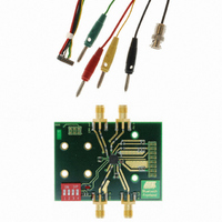
Manufacturer Part Number
DEMOBOARD-T7024PGM
Description
BOARD DEMO FOR T7024PGM
Manufacturer
Atmel
Type
Bluetoothr
Specifications of DEMOBOARD-T7024PGM
Frequency
2.4GHz
Processor Series
T7024
Wireless Frequency
2.4 GHz
For Use With/related Products
T7024PGM
Lead Free Status / RoHS Status
Contains lead / RoHS non-compliant
Other names
DEMOBOARD-T7024-PGM


Power Amplifier
The power amplifier of the T7024 is designed as a three-stage amplifier. The input stage
of the amplifier is AC-coupled to PA_IN. Therefore, a DC blocking capacitor is not nec-
essary at the input port. An external matching circuit should however be designed for
optimum performance of the power amplifier. The power amplifier has a nominal input
power of 0 dBm. It is therefore recommended that the input circuit should be designed at
this value. This has been done for the matching circuits on the application boards. The
difference between the input matching circuits for the T7024 in PSSO20 package and
the T7024 in QFN20 package result from the fact that the RF performance changes with
the different packages.
The power amplifier of the T7024 is turned on and off with the ramp input signal.
It is very important that the slug on the backside of the IC has a good connection to RF
ground.
The supply voltage for the collector of the first amplifier stage is connected via V1_PA.
Since the collector is internally matched to simplify the handling, an additional matching
is recommended. The supply line for the matching is not very sensitive in terms of output
power and PAE.
The supply voltage for the collector of the second stage is fed using a 50
transmission
line. In both reference designs, a capacitor of 3.3 pF with a high Q value should be
placed close to the two IC pins. The RF blocking of this stage with the 15 pF capacitor is
done after a length of approximately 10 mm to 15 mm using a 50
transmission line.
The matching for the second stage is sensitive. The blocking capacitors should be
placed with some distance to the matching capacitor of 3.3 pF, otherwise output power
and PAE will drop. Since the matching capacitor (and its resonant frequency) has great
influence on the output power, it may be useful to consider using slightly different values
(3.0 pF to 3.6 pF), since the exact capacitance and the parasitic influence vary depend-
ing on manufacturer and size.
Finally, the third stage uses three output connectors for the open collector. In the refer-
ence design for the PSSO20 package, it is recommended that one short stub with a
length of 1 mm should be used as a harmonic termination. This harmonic termination is
not necessary to achieve the output power, however, a shorting of the second harmonic
reduces RF losses in the output transistor and therefore increases the power added effi-
ciency (PAE). The other two output connectors (pin 7 and pin 8) are connected to each
other. For the output matching, a capacitor of 0.8 pF to ground and a DC blocking
capacitor of 1.5 pF should be used. Make sure that the capacitor to ground is placed
very close to the RF output pins. The DC feeding inductor of 15 nH should also be
placed near the RF output.
For the output matching, a capacitor of 0.8 pF to ground and a DC blocking capacitor of
2.2 pF should be used. Make sure that the capacitor to ground and the DC blocking
capacitor are placed very close to the RF output connector. Finally, the DC feeding
inductor of 18 nH should also be placed near the RF output pin 11.
Since the two capacitors play the major role for a good match to 50
for both reference
designs, it is recommended that capacitors with a high Q factor are used.
As harmonic terminations, the reference design for the QFN20 package uses actually
two short stubs with 1 mm length.
Design Guide T7024
6
4549D–BLURF–06/04
Related parts for DEMOBOARD-T7024PGM
Image
Part Number
Description
Manufacturer
Datasheet
Request
R

Part Number:
Description:
BOARD DEMO FOR U4091BM
Manufacturer:
Atmel
Datasheet:


Part Number:
Description:
BOARD DEMO FOR U3600BM
Manufacturer:
Atmel
Datasheet:

Part Number:
Description:
BOARD DEMO FOR ATR2806
Manufacturer:
Atmel
Datasheet:
Part Number:
Description:
BOARD DEMO COM-I/Q MOD 1GHZ
Manufacturer:
Atmel
Datasheet:

Part Number:
Description:
Banana & Binding Post Connectors SINGLE PCB SOCK BLK
Manufacturer:
DEM Manufacturing
Datasheet:
Part Number:
Description:
Banana & Binding Post Connectors PLUG RED
Manufacturer:
DEM Manufacturing
Datasheet:
Part Number:
Description:
Banana & Binding Post Connectors SINGLE PCB SOCK RED
Manufacturer:
DEM Manufacturing
Datasheet:
Part Number:
Description:
DIN Connectors SOCKET NICKEL 8 PIN
Manufacturer:
DEM Manufacturing
Datasheet:
Part Number:
Description:
DIN Connectors PLUG NICKEL 3 PIN
Manufacturer:
DEM Manufacturing
Datasheet: