DEMOBOARD-T7024PGM Atmel, DEMOBOARD-T7024PGM Datasheet - Page 16
DEMOBOARD-T7024PGM
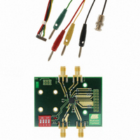
Manufacturer Part Number
DEMOBOARD-T7024PGM
Description
BOARD DEMO FOR T7024PGM
Manufacturer
Atmel
Type
Bluetoothr
Specifications of DEMOBOARD-T7024PGM
Frequency
2.4GHz
Processor Series
T7024
Wireless Frequency
2.4 GHz
For Use With/related Products
T7024PGM
Lead Free Status / RoHS Status
Contains lead / RoHS non-compliant
Other names
DEMOBOARD-T7024-PGM


Frequently Asked
Questions
16
Design Guide T7024
1. What is the advantage of SiGe Hetero Junction Transistor Technology?
There are several advantages:
•
•
•
•
2. What is the maximum allowed voltage for V
3. What is the typical gain partitioning of three stage power amplifier T7024?
4. Is there a chronological order to be obeyed when connecting the PA to power
5. Is it possible to make a short circuit at the RF input or output terminal during
6. Is it possible to make a short circuit at the Vcc terminals of the PA during opera-
7. What is the purpose of interstage matching?
The silicon material itself has a 3 times higher thermal conductivity compared to
GaAs material which leads to a much better thermal dissipation of the heat that is
generated in the transistor cells.
For both bipolar and GaAs transistors an increased beta can be observed with
increased device temperature. This leads to higher current and finally to destruction
of the transistor. For SiGe devices, there is a decreasing of beta with temperature
and therefore a built-in self-stabilization of the transistor cell itself.
Due to the negligible quiescent current, there is no need for the high side switch
transistor normally required by GaAs's even for large transistor structures.
All necessary circuitry for proper operation of RF power cells (band gap, biasing,
ramp voltage generation, temperature compensation a. s. o.) are normally
integrated into the main chip.
V
V
1
2
3
The decreasing gain per stage is due to the size of the stage and the losses in the
interstage matching.
supply?
Yes, first, make sure that all RF terminals (i.e. RF input and output) are terminated
with 50 Ohms. After that, all V
supply and switched on. Then an RF input signal within the frequency range and
power range specified in the data sheet has to be applied to the PA input. After that,
Vramp can be applied and is used to adjust the RF output power to the desired
level.
operation?
No, this is strictly forbidden. It is possible to apply a certain mismatch at the output
terminal of the PA, but for the exact values and conditions please refer to the data
sheet.
tion or shortly after operation?
No, we don't recommend to apply a short circuit to the terminals of PA, because
- depending on application circuit - there might arise strong voltage peaks due to
inductors or other inductive components like feeding lines in the supply chain.
These voltages may reach up to 3 times the standard voltage levels and can be
measured only with a very fast oscilloscope.
The input and output impedance of a single power amplifier stage has to be
matched to the impedance of the preceding or following stages respectively. This is
done to avoid spurious or unwanted oscillations and to reduce the gain loss due to
mismatch.
st
nd
rd
cbo
ceo
stage: ~12 dB
stage: ~9 dB
stage: ~11 dB
(max) = 15 V
(max) = 5.5 V
cc
terminals and grounds need to be connected to the
cbo
and V
ceo
?
4549D–BLURF–06/04
Related parts for DEMOBOARD-T7024PGM
Image
Part Number
Description
Manufacturer
Datasheet
Request
R

Part Number:
Description:
BOARD DEMO FOR U4091BM
Manufacturer:
Atmel
Datasheet:


Part Number:
Description:
BOARD DEMO FOR U3600BM
Manufacturer:
Atmel
Datasheet:

Part Number:
Description:
BOARD DEMO FOR ATR2806
Manufacturer:
Atmel
Datasheet:
Part Number:
Description:
BOARD DEMO COM-I/Q MOD 1GHZ
Manufacturer:
Atmel
Datasheet:

Part Number:
Description:
Banana & Binding Post Connectors SINGLE PCB SOCK BLK
Manufacturer:
DEM Manufacturing
Datasheet:
Part Number:
Description:
Banana & Binding Post Connectors PLUG RED
Manufacturer:
DEM Manufacturing
Datasheet:
Part Number:
Description:
Banana & Binding Post Connectors SINGLE PCB SOCK RED
Manufacturer:
DEM Manufacturing
Datasheet:
Part Number:
Description:
DIN Connectors SOCKET NICKEL 8 PIN
Manufacturer:
DEM Manufacturing
Datasheet:
Part Number:
Description:
DIN Connectors PLUG NICKEL 3 PIN
Manufacturer:
DEM Manufacturing
Datasheet: