AMMC-5033-W10 Avago Technologies US Inc., AMMC-5033-W10 Datasheet
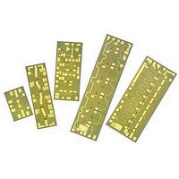
IC MMIC AMP GAAS 17.7-32GHZ

AMMC-5033-W10

Manufacturer Part Number
AMMC-5033-W10
Description
IC MMIC AMP GAAS 17.7-32GHZ
Manufacturer
Avago Technologies US Inc.
Type
Power Amplifierr
Datasheet

Specifications of AMMC-5033-W10

Function
Amplifier
Gain
20dB
Supply Current
280mA
Supply Voltage Range
3.5V, 5V
Frequency Max
32GHz
Frequency Min
17.7GHz
Supply Voltage Max
7V
Number Of Channels
1
Frequency (max)
32GHz
Output Power
26.5@32000MHzdBm
Power Supply Requirement
Single
Single Supply Voltage (max)
7V
Package Type
Chip
Dual Supply Voltage (min)
Not RequiredV
Dual Supply Voltage (typ)
Not RequiredV
Dual Supply Voltage (max)
Not RequiredV
Lead Free Status / RoHS Status
Lead free / RoHS Compliant
Lead Free Status / RoHS Status
Lead free / RoHS Compliant, Lead free / RoHS Compliant

Available stocks

Company
Part Number
Manufacturer
Quantity
Price
Part Number:
AMMC-5033-W10
Manufacturer:
TriQuint
Quantity:
5 000
Part Number:
AMMC-5033-W10
Manufacturer:
AVAGO/安华高
Quantity:
20 000
AMMC-5033
17.7 - 32 GHz Power Amplifier
Data Sheet
Description
Avago’s AMMC-5033 is a MMIC power amplifier designed
for use in wireless transmitters that operate within
17.7 GHz to 32 GHz range. At 25 GHz, it provides 27 dBm
of output power (P-1dB) and 20 dB of small- signal gain
from a small easy-to-use device. The device has input
and output matching circuitry for use in 50 Ω environ-
ments. The AMMC- 5033 also integrates a temperature
compensated RF power detection circuit that enables
power detection of 0.1 V/W at 22 GHz. For improved
reliability and moisture protection, the die is passivated
at the active areas.
AMMC-5033 Absolute Maximum Ratings
Symbol
V
V
Det Bias
I
I
P
T
T
T
Note:
1. Operation in excess of any one of these conditions may result
d1
d2
ch
stg
max
d1,2
in
g1
in permanent damage to this device.
, V
gg
Note: These devices are ESD sensitive. The following precautions are strongly recommended:
Ensure that an ESD approved carrier is used when dice are transported from one destination to another.
Personal grounding is to be worn at all times when handling these devices.
Parameters/Conditions
Positive Drain Voltage
Gate Supply Voltage
Applied Detector Bias
(Optional)
First Stage Drain Current
Second Stage Drain Current
CW Input Power
Operating Channel Temp.
Storage Case Temp.
Maximum Assembly Temp.
(60 sec max)
Units
V
V
V
mA
mA
dBm
°C
°C
°C
[1]
Min. Max.
-3
-65
7
0.5
7
320
640
23
+150
+150
+300
Features
• Wide frequency range: 17.7 – 32 GHz
• High power: P-1dB @ 25 GHz = 27 dBm
• High gain: 20 dB
• Return loss: Input: -13 dB, Output: –20 dB
• Integrated RF power detector
Applications
• Designed for use in transmitters that operate in various
• Can be driven by the AMMC-5040 (20-40 GHz) or the
Chip Size: 2730 x 1300 µm (108 x 51.6 mils)
Chip Size Tolerance: ± 10 µm (±0.4 mils)
Chip Thickness: 100 ± 10 µm (4 ± 0.4 mils)
Pad Dimensions: 80 x 80 µm (2.95 ± 0.4 mils)
frequency bands between 17.7 GHz and 32 GHz.
AMMC-5618 (6-20 GHz) MMIC amplifiers, increasing
the power handling capability of transmitters requiring
linear operation.

Related parts for AMMC-5033-W10

AMMC-5033-W10 Summary of contents

Page 1

... Integrated RF power detector Applications • Designed for use in transmitters that operate in various frequency bands between 17.7 GHz and 32 GHz. • Can be driven by the AMMC-5040 (20-40 GHz) or the AMMC-5618 (6-20 GHz) MMIC amplifiers, increasing [1] the power handling capability of transmitters requiring Units Min ...

Page 2

... AMMC-5033 DC Specifications/Physical Properties Symbol Parameters and Test Conditions I First Stage Drain Supply Current 3 Open Second Stage Drain Supply Current Open Vgg Gate Supply Operating Voltage ( 780 (mA)) d1(Q) d2(Q) DETBias Detector Bias Voltage (Optional) θ First Stage Thermal Resistance c1(ch-bs) (Backside Temperature 25°C) θ ...

Page 3

... AMMC-5033 Typical Performances (T = 25° 3 280 mA S21 (dB) 35 S12 (dB - FREQUENCY (GHz) Figure 1. Gain and reverse isolation P FREQUENCY (GHz) Figure 3. Output power and 3 dB gain compression FREQUENCY (GHz) Figure 5. Output 3rd order intercept point 500 mA Ω out 0 -5 -10 ...

Page 4

... AMMC-5033 Typical Performance Curves (Over Temperature and Voltage) 0.10 0.08 0.06 0.04 0.02 0. Output Power (dBm) Figure 6. Linear and log detector voltage and output power, freq GHz, Det_B = 5V/0.5A 22 4V/0.5 3.5V/0. FREQUENCY (GHz) Figure 8. Output power gain compression and V voltage 3.5 V (constant) ...

Page 5

- FREQUENCY (GHz) Figure 10. Output power gain compression and temperature ...

Page 6

Typical Scattering Parameters [ 25° 3 280 mA Freq S11 [GHz] dB Mag Phase dB 1 -10.7 0.29 173 -51.1 2 -11.0 0.28 167 -70.1 3 -11.4 0.27 161 ...

Page 7

... No ground wires are needed since ground connections are made with plated through-holes to the backside of the device. 7 Assembly Techniques The backside of the AMMC- 5033 chip is RF ground. For microstripline applications, the chip should be attached set for directly to the ground plane (e.g., circuit carrier or heat ...

Page 8

... Vgg GND Input 50 250 1000 V GND Figure 13. AMMC-5033 schematic Figure 14. AMMC-5033 bonding pad locations, dimensions are in microns GND d2 DET _ . OUT OUT DET _ . BIAS Ref_ D 2 DET _ . REF 50 V GND DQ d2 ...

Page 9

... EE Figure 15. AMMC-5033 assembly diagram Ordering Information: AMMC-5033-W10 = 10 devices per tray AMMC-5033-W50 = 50 devices per tray For product information and a complete list of distributors, please go to our website: Avago, Avago Technologies, and the A logo are trademarks of Avago Technologies Limited in the United States and other countries. ...

Related keywords