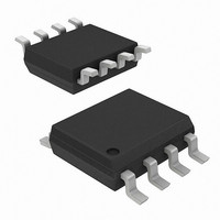
AD8361ARMZ Analog Devices Inc, AD8361ARMZ Datasheet - Page 17

AD8361ARMZ
Manufacturer Part Number
AD8361ARMZ
Description
IC PWR DETECTOR 2.5GHZ 8-MSOP
Manufacturer
Analog Devices Inc
Datasheet
1.AD8361-EVAL.pdf
(24 pages)
Specifications of AD8361ARMZ
Rf Type
Cellular, CDMA, W-CDMA
Frequency
100MHz ~ 2.5GHz
Input Range
0 ~ 700mV
Accuracy
±0.25dB
Voltage - Supply
2.7 V ~ 5.5 V
Current - Supply
1.1mA
Package / Case
8-TSSOP, 8-MSOP (0.118", 3.00mm Width)
Frequency Range
100MHz To 2.5GHz
Supply Current
1.1mA
Supply Voltage Range
2.7V To 5.5V
Rf Ic Case Style
MSOP
No. Of Pins
8
Operating Temperature Range
-40°C To +85°C
Pin Count
8
Screening Level
Industrial
Package Type
MSOP
Lead Free Status / RoHS Status
Lead free / RoHS Compliant
Lead Free Status / RoHS Status
Lead free / RoHS Compliant, Lead free / RoHS Compliant
Available stocks
Company
Part Number
Manufacturer
Quantity
Price
Company:
Part Number:
AD8361ARMZ
Manufacturer:
ADI
Quantity:
3 000
Company:
Part Number:
AD8361ARMZ
Manufacturer:
SOP8
Quantity:
4 800
Part Number:
AD8361ARMZ
Manufacturer:
ADI/亚德诺
Quantity:
20 000
Company:
Part Number:
AD8361ARMZ-REEL
Manufacturer:
AD
Quantity:
5 510
Company:
Part Number:
AD8361ARMZ-REEL
Manufacturer:
AMI
Quantity:
5 510
Part Number:
AD8361ARMZ-REEL
Manufacturer:
ADI/亚德诺
Quantity:
20 000
Company:
Part Number:
AD8361ARMZ-REEL7
Manufacturer:
STANLEY
Quantity:
12 000
Part Number:
AD8361ARMZ-REEL7
Manufacturer:
ADI/亚德诺
Quantity:
20 000
Part Number:
AD8361ARMZ-RL7
Manufacturer:
ADI/亚德诺
Quantity:
20 000
The equation can be rewritten to yield a temperature
compensated value for V
Figure 52 shows the output voltage and error (in dB) as a
function of input level for a typical device (note that output
voltage is plotted on a logarithmic scale). Figure 53 shows the
error in the calculated input level after the temperature
compensation algorithm has been applied. For a supply voltage
of 5 V, the part exhibits a worst-case linearity error over
temperature of approximately ±0.3 dB over a dynamic range of
35 dB.
–0.5
–1.0
–1.5
–2.0
–2.5
2.5
2.0
1.5
1.0
0.5
V
0
–0.5
–1.0
–1.5
–2.0
–2.5
–3.0
–25
2.0
1.5
1.0
0.5
IN
0
–30
=
Figure 53. Error after Temperature Compensation of
(
V
–20
Figure 52. Typical Output Voltage and Error vs.
OUT
–25
+25°C
Output Reference,800 MHz, V
−
Input Level, 800 MHz, VPOS = 5 V
V
–15
–20
OS
+85°C
−
IN
DRIFT
–15
–10
:
PIN (dBm)
+25°C
GAIN
PIN (dBm)
VOS
–10
–5
×
(
TEMP
–5
–40°C
+85°C
0
POS
–40°C
= 5 V
−
0
25°
5
C
)
5
)
10
10
1.0
0.1
10
Rev. C | Page 17 of 24
Extended Frequency Characterization
Although the AD8361 was originally intended as a power
measurement and control device for cellular wireless
applications, the AD8361 has useful performance at higher
frequencies. Typical applications may include MMDS, LMDS,
WLAN, and other noncellular activities.
In order to characterize the AD8361 at frequencies greater than
2.5 GHz, a small collection of devices were tested. Dynamic
range, conversion gain, and output intercept were measured at
several frequencies over a temperature range of −30°C to +80°C.
Both CW and 64 QAM modulated input wave forms were used
in the characterization process in order to access varying peak-
to-average waveform performance.
The dynamic range of the device is calculated as the input
power range over which the device remains within a
permissible error margin to the ideal transfer function. Devices
were tested over frequency and temperature. After identifying
an acceptable error margin for a given application, the usable
dynamic measurement range can be identified using the plots in
Figure 54 through Figure 57. For instance, for a 1 dB error
margin and a modulated carrier at 3 GHz, the usable dynamic
range can be found by inspecting the 3 GHz plot of Figure 57.
Note that the −30°C curve crosses the −1 dB error limit at
−17 dBm. For a 5 V supply, the maximum input power should
not exceed 6 dBm in order to avoid compression. The resultant
usable dynamic range is therefore
or 23 dBm over a temperature range of −30°C to +80°C.
–0.5
–1.0
–1.5
–2.0
–2.5
2.5
2.0
1.5
1.0
0.5
6 dBm − (−17 dBm)
0
–25
Figure 54. Transfer Function and Error Plots Measured at
–20
–30°C
1.5 GHz for a 64 QAM Modulated Signal
–15
+25°C
–10
PIN (dBm)
+80°C
–5
0
5
AD8361
10
10
1
0.1


