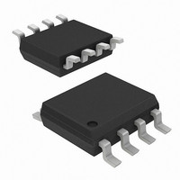
AD8361ARMZ Analog Devices Inc, AD8361ARMZ Datasheet - Page 15

AD8361ARMZ
Manufacturer Part Number
AD8361ARMZ
Description
IC PWR DETECTOR 2.5GHZ 8-MSOP
Manufacturer
Analog Devices Inc
Datasheet
1.AD8361-EVAL.pdf
(24 pages)
Specifications of AD8361ARMZ
Rf Type
Cellular, CDMA, W-CDMA
Frequency
100MHz ~ 2.5GHz
Input Range
0 ~ 700mV
Accuracy
±0.25dB
Voltage - Supply
2.7 V ~ 5.5 V
Current - Supply
1.1mA
Package / Case
8-TSSOP, 8-MSOP (0.118", 3.00mm Width)
Frequency Range
100MHz To 2.5GHz
Supply Current
1.1mA
Supply Voltage Range
2.7V To 5.5V
Rf Ic Case Style
MSOP
No. Of Pins
8
Operating Temperature Range
-40°C To +85°C
Pin Count
8
Screening Level
Industrial
Package Type
MSOP
Lead Free Status / RoHS Status
Lead free / RoHS Compliant
Lead Free Status / RoHS Status
Lead free / RoHS Compliant, Lead free / RoHS Compliant
Available stocks
Company
Part Number
Manufacturer
Quantity
Price
Company:
Part Number:
AD8361ARMZ
Manufacturer:
ADI
Quantity:
3 000
Company:
Part Number:
AD8361ARMZ
Manufacturer:
SOP8
Quantity:
4 800
Part Number:
AD8361ARMZ
Manufacturer:
ADI/亚德诺
Quantity:
20 000
Company:
Part Number:
AD8361ARMZ-REEL
Manufacturer:
AD
Quantity:
5 510
Company:
Part Number:
AD8361ARMZ-REEL
Manufacturer:
AMI
Quantity:
5 510
Part Number:
AD8361ARMZ-REEL
Manufacturer:
ADI/亚德诺
Quantity:
20 000
Company:
Part Number:
AD8361ARMZ-REEL7
Manufacturer:
STANLEY
Quantity:
12 000
Part Number:
AD8361ARMZ-REEL7
Manufacturer:
ADI/亚德诺
Quantity:
20 000
Part Number:
AD8361ARMZ-RL7
Manufacturer:
ADI/亚德诺
Quantity:
20 000
The filter capacitance of the AD8361 can be augmented by
connecting a capacitor between Pin 6 (FLTR) and VPOS. Table 7
shows the effect of several capacitor values for various
communications standards with high peak-to-average ratios
along with the residual ripple at the output, in peak-to-peak and
rms volts. Note that large filter capacitors increase the enable and
pulse response times, as discussed below.
Table 7. Effect of Waveform and CFILT on Residual AC
Waveform
IS95 Reverse Link
IS95 8-Channel
W-CDMA 15
Operation at Low Frequencies
Although the AD8361 is specified for operation up to 2.5 GHz,
there is no lower limit on the operating frequency. It is only
necessary to increase the input coupling capacitor to reduce the
corner frequency of the input high-pass filter (use an input
resistance of 225 Ω for frequencies below 100 MHz). It is also
necessary to increase the filter capacitor so that the signal at the
output of the squaring circuit is free of ripple. The corner
frequency is set by the combination of the internal resistance of
2 kΩ and the external filter capacitance.
Power Consumption, Enable and Power-On
The quiescent current consumption of the AD8361 varies with
the size of the input signal from about 1 mA for no signal up to
7 mA at an input level of 0.66 V rms (9.4 dBm, re 50 Ω). If the
input is driven beyond this point, the supply current increases
steeply (see Figure 16). There is little variation in quiescent
current with power supply voltage.
The AD8361 can be disabled either by pulling the PWDN
(Pin 4) to VPOS or by simply turning off the power to the
device. While turning off the device obviously eliminates the
Forward Link
Channel
C
Open
0.01 µF
0.1 µF
0.01 µF
0.1 µF
0.01 µF
0.1 µF
FILT
Output
V dc
0.5
1.0
2.0
0.5
1.0
2.0
0.5
1.0
2.0
0.5
1.0
2.0
0.5
1.0
2.0
0.5
1.0
2.0
0.5
1.0
2.0
mV p-p
550
1000
2000
40
160
430
20
40
110
290
975
2600
50
190
670
225
940
2500
45
165
550
Residual AC
mV rms
100
180
360
6
20
60
3
6
18
40
430
7
30
95
35
135
390
6
25
80
150
Rev. C | Page 15 of 24
current consumption, disabling the device reduces the leakage
current to less than 1 µA. Figure 27 and Figure 28 show the
response of the output of the AD8361 to a pulse on the PWDN
pin, with no capacitance and with a filter capacitance of 0.01 µF,
respectively; the turn-on time is a function of the filter
capacitor. Figure 31 shows a plot of the output response to the
supply being turned on (i.e., PWDN is grounded and VPOS is
pulsed) with a filter capacitor of 0.01 µF. Again, the turn-on
time is strongly influenced by the size of the filter capacitor.
If the input of the AD8361 is driven while the device is disabled
(PWDN = VPOS), the leakage current of less than 1 µA
increases as a function of input level. When the device is
disabled, the output impedance increases to approximately
16 kΩ.
Volts to dBm Conversion
In many of the plots, the horizontal axis is scaled in both rms
volts and dBm. In all cases, dBm are calculated relative to an
impedance of 50 Ω. To convert between dBm and volts in a
50 Ω system, the following equations can be used. Figure 48
shows this conversion in graphical form.
V
Power
rms
=
(
dBm
Figure 48. Conversion from dBm to rms Volts
0.001
)
=
10log
W
0.001
0.01
0.1
×
1
V rms
50
⎡
⎢
⎢
⎢
⎢
⎢
⎣
(
0.001
Ω
V
50
×
rms
log
Ω
dBm
W
)
2
−
1
–10
–20
–30
⎤
⎥
⎥
⎥
⎥
⎥
⎦
+20
+10
0
–40
⎛
⎜
⎝
=
dBm
10
10log
⎞
⎟
⎠
=
(
20
(
log
V
rms
AD8361
−
1
(
dBm
20
)
2
)
/10
)


