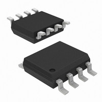
AD8361ARMZ Analog Devices Inc, AD8361ARMZ Datasheet - Page 13

AD8361ARMZ
Manufacturer Part Number
AD8361ARMZ
Description
IC PWR DETECTOR 2.5GHZ 8-MSOP
Manufacturer
Analog Devices Inc
Datasheet
1.AD8361-EVAL.pdf
(24 pages)
Specifications of AD8361ARMZ
Rf Type
Cellular, CDMA, W-CDMA
Frequency
100MHz ~ 2.5GHz
Input Range
0 ~ 700mV
Accuracy
±0.25dB
Voltage - Supply
2.7 V ~ 5.5 V
Current - Supply
1.1mA
Package / Case
8-TSSOP, 8-MSOP (0.118", 3.00mm Width)
Frequency Range
100MHz To 2.5GHz
Supply Current
1.1mA
Supply Voltage Range
2.7V To 5.5V
Rf Ic Case Style
MSOP
No. Of Pins
8
Operating Temperature Range
-40°C To +85°C
Pin Count
8
Screening Level
Industrial
Package Type
MSOP
Lead Free Status / RoHS Status
Lead free / RoHS Compliant
Lead Free Status / RoHS Status
Lead free / RoHS Compliant, Lead free / RoHS Compliant
Available stocks
Company
Part Number
Manufacturer
Quantity
Price
Company:
Part Number:
AD8361ARMZ
Manufacturer:
ADI
Quantity:
3 000
Company:
Part Number:
AD8361ARMZ
Manufacturer:
SOP8
Quantity:
4 800
Part Number:
AD8361ARMZ
Manufacturer:
ADI/亚德诺
Quantity:
20 000
Company:
Part Number:
AD8361ARMZ-REEL
Manufacturer:
AD
Quantity:
5 510
Company:
Part Number:
AD8361ARMZ-REEL
Manufacturer:
AMI
Quantity:
5 510
Part Number:
AD8361ARMZ-REEL
Manufacturer:
ADI/亚德诺
Quantity:
20 000
Company:
Part Number:
AD8361ARMZ-REEL7
Manufacturer:
STANLEY
Quantity:
12 000
Part Number:
AD8361ARMZ-REEL7
Manufacturer:
ADI/亚德诺
Quantity:
20 000
Part Number:
AD8361ARMZ-RL7
Manufacturer:
ADI/亚德诺
Quantity:
20 000
Dynamic Range
Because the AD8361 is a linear-responding device with a
nominal transfer function of 7.5 V/V rms, the dynamic range in
dB is not clear from plots such as Figure 39. As the input level is
increased in constant dB steps, the output step size (per dB) also
increases. Figure 41 shows the relationship between the output
step size (i.e., mV/dB) and input voltage for a nominal transfer
function of 7.5 V/V rms.
Table 4. Connections and Nominal Transfer Function for
Ground, Internal, and Supply Reference Modes
Reference
Mode
Ground
Internal
Supply
Plots of output voltage versus input voltage result in a straight
line. It may sometimes be more useful to plot the error on a
logarithmic scale, as shown in Figure 42. The deviation of the
plot for the ideal straight line characteristic is caused by output
clipping at the high end and by signal offsets at the low end. It
Figure 41. Idealized Output Step Size as a Function of Input Voltage
700
600
500
400
300
200
100
5.5
5.0
4.5
4.0
3.5
3.0
2.5
2.0
1.5
1.0
0.5
0.0
0
0
0
Figure 40. Output Swing for Supply Voltages of
100
0.1
IREF
VPOS
OPEN
VPOS
2.7 V, 3.0 V, 5.0 V and 5.5 V (MSOP Only)
200
0.2
SREF
COMM
COMM
VPOS
300
0.3
INPUT (V rms)
INPUT (mV)
400
0.4
Output
Intercept
(No Signal)
Zero
0.350 V
V
S
/7.5
500
0.5
2.7V
5.5V
600
0.6
3.0V
Output
7.5 V
7.5 V
7.5 V
700
0.7
5.0V
IN
IN
IN
+ 0.350 V
+ V
800
0.8
S
/7.5
Rev. C | Page 13 of 24
should however be noted that offsets at the low end can be
either positive or negative, so this plot could also trend upwards
at the low end. Figure 9, Figure 10, Figure 12, and Figure 13
show a ±3 sigma distribution of the device error for a large
population of devices.
It is also apparent in Figure 42 that the error plot tends to shift
to the right with increasing frequency. Because the input
impedance decreases with frequency, the voltage actually
applied to the input also tends to decrease (assuming a constant
source impedance over frequency). The dynamic range is
almost constant over frequency, but with a small decrease in
conversion gain at high frequency.
Input Coupling and Matching
The input impedance of the AD8361 decreases with increasing
frequency in both its resistive and capacitive components
(Figure 17). The resistive component varies from 225 Ω at
100 MHz down to about 95 Ω at 2.5 GHz.
A number of options exist for input matching. For operation at
multiple frequencies, a 75 Ω shunt to ground, as shown in
Figure 43, provides the best overall match. For use at a single
frequency, a resistive or a reactive match can be used. By
plotting the input impedance on a Smith Chart, the best value
for a resistive match can be calculated. The VSWR can be held
below 1.5 at frequencies up to 1 GHz, even as the input
impedance varies from part to part. (Both input impedance and
input capacitance can vary by up to ±20% around their nominal
values.) At very high frequencies (i.e., 1.8 GHz to 2.5 GHz), a
shunt resistor is not sufficient to reduce the VSWR below 1.5.
Where VSWR is critical, remove the shunt component and
insert an inductor in series with the coupling capacitor as
shown in Figure 44.
Table 5 gives recommended shunt resistor values for various
frequencies and series inductor values for high frequencies. The
coupling capacitor, C
no intentional part in the matching.
Figure 42. Representative Unit, Error in dB vs. Input Level, V
–0.5
–1.0
–1.5
–2.0
1.5
1.0
2.0
0.5
0.0
0.01
(–21dBm)
100MHz
0.02
C
, essentially acts as an ac-short and plays
INPUT (V rms)
(–7dBm)
0.1
100MHz
900MHz
(+5dBm)
0.4
2.5GHz
1.9GHz
AD8361
S
= 2.7 V
1.0


