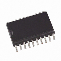
U2794B-MFSG3 Atmel, U2794B-MFSG3 Datasheet - Page 5

U2794B-MFSG3
Manufacturer Part Number
U2794B-MFSG3
Description
IC DEMODULATR QUAD 1K MHZ 20SOIC
Manufacturer
Atmel
Datasheet
1.U2794B-NFSG3H.pdf
(15 pages)
Specifications of U2794B-MFSG3
Function
Demodulator
Lo Frequency
70MHz ~ 1GHz
Rf Frequency
40MHz ~ 1.03GHz
P1db
3.5dBm
Noise Figure
12dB
Current - Supply
35mA
Voltage - Supply
4.75 V ~ 5.25 V
Package / Case
20-SOIC (0.200", 5.30mm Width)
Lead Free Status / RoHS Status
Lead free / RoHS Compliant
Gain
-
6. Electrical Characteristics (Continued)
Test conditions (unless otherwise specified); V
System impedance Z
4653F–CELL–11/08
7.5
7.6
7.7
*) Type means: A = 100% tested, B = 100% correlation tested, C = Characterized on samples, D = Design parameter
Notes:
No.
6.1
6.2
6.3
6.4
6.5
6.6
6.7
7.1
7.2
7.3
7.4
6
7
Parameters
I/Q Outputs (I, IX, Q, QX) Emitter Follower I = 0.6 mA
3-dB bandwidth
w/o external C
I/Q amplitude error
I/Q phase error
I/Q maximum output
swing
DC output voltage
DC output offset
voltage
Output impedance
Gain Control, GC
Control range power
Gain high
Gain low
Switch Voltage
“Gain high”
“Gain low”
Settling Time, ST
Power “OFF” - “ON”
Power “ON” - “OFF”
1. During power-down status a load circuitry with DC-isolation to GND is assumed, otherwise a current of I
2. The required LO-Level is a function of the LO frequency (see
3. Measured with input matching. For 950 MHz, the optional transmission line T3 at the RF input may be used for this pur-
4. Using pins 7 and 8 as a symmetric RF input, the second-order IIP can be improved.
5. Due to test board parasitics, this bandwidth may be reduced and not be equal for I, IX, Q, QX. If symmetry and full band-
6. The internal current of the output emitter followers is 0.6 mA. This reduces the undistorted output voltage swing at a 50
7. Referred to the level of the output vector
8. The low-gain status is achieved with an open or high-ohmic pin 11. A recommended application circuit for switching
has to be added to the above power-down current for each output I, IX, Q, QX.
pose. Noise figure measurements without using the differential output signal result in a worse noise figure.
width is required, the lowpass pins 3, 4 and 9, 10 should be isolated from the board. the bandwidth of the I/Q outputs can
be increased further by using a resistor between pins 3, 4, 9 and 10. These resistors shunt the internal loads of
RI ~ 5.4 k . The decrease in gain here has to be considered.
load to approximately 30 mV. For low signal distortion the load impedance should be RI
between high and low gain status is shown in
O
= 50 , f
iLO
= 950 MHz, P
Test Conditions
Symm. output
R
(6)
see
(7)
(8)
L
> 5 k
Figure 6-10
S
iLO
= 5V, T
= –10 dBm
amb
I
2
= 25°C, referred to test circuit
11 < open
+
1, 2, 19,
1, 2, 19,
1, 2, 19,
1, 2, 19,
1, 2, 19,
1, 2, 19,
1, 2, 19,
Figure
Q
Pin
20
20
20
20
20
20
20
11
11
2
6-1.
Symbol
BWI/Q
T
V
GCR
V
T
Figure
V
Z
Ae
G
SOFF
Pe
offset
G
OUT
SON
out
PP
H
L
6-6).
Min.
–0.5
2.5
–3
30
Typ.
2.8
< 5
< 4
< 4
±0.2
50
25
23
–2
±1.5
5 k .
Max.
+0.5
3.1
+3
2
1
MHz
U2794B
Unit
Deg
mV
dB
dB
dB
dB
(VS –0.8V)/RI
µs
µs
V
V
Type*
spec.
Test
D
B
B
D
A
D
D
B
D
D
D
5


