MW5IC970NBR1 Freescale Semiconductor, MW5IC970NBR1 Datasheet - Page 2
MW5IC970NBR1
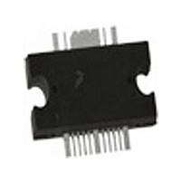
Manufacturer Part Number
MW5IC970NBR1
Description
IC PWR AMP RF 28V 70W TO-272-16
Manufacturer
Freescale Semiconductor
Type
Power Amplifierr
Specifications of MW5IC970NBR1
Current - Supply
80mA
Frequency
800MHz ~ 900MHz
Gain
30dB
Package / Case
TO-272-16
Rf Type
General Purpose
Voltage - Supply
28V
Number Of Channels
1
Frequency (max)
900MHz
Power Supply Requirement
Single
Single Supply Voltage (typ)
28V
Dual Supply Voltage (min)
Not RequiredV
Dual Supply Voltage (typ)
Not RequiredV
Dual Supply Voltage (max)
Not RequiredV
Pin Count
16
Mounting
Surface Mount
Lead Free Status / RoHS Status
Lead free / RoHS Compliant
Noise Figure
-
P1db
-
Test Frequency
-
Lead Free Status / Rohs Status
Compliant
Available stocks
Company
Part Number
Manufacturer
Quantity
Price
Company:

Part Number:
MW5IC970NBR1
Manufacturer:
ZCOMM
Quantity:
1 400
Part Number:
MW5IC970NBR1
Manufacturer:
FREESCALE
Quantity:
20 000


MW5IC970NBR1 MW5IC970GNBR1
2
Table 1. Maximum Ratings
Table 2. Thermal Characteristics
Table 3. ESD Protection Characteristics
Table 4. Moisture Sensitivity Level
Table 5. Electrical Characteristics
Functional Tests (In Freescale Test Fixture, 50 ohm system) V
f1 = 870.0 MHz, f2 = 870.1 MHz
Typical 800/900 MHz Performances (In Freescale 800/900 MHz Reference Fixture, 50 ohm system) V
650 mA, 740-870 MHz, 870-960 MHz
Drain-Source Voltage
Gate-Source Voltage
Storage Temperature Range
Case Operating Temperature
Operating Junction Temperature
Thermal Resistance, Junction to Case
Human Body Model (per JESD22-A114)
Machine Model (per EIA/JESD22-A115)
Charge Device Model (per JESD22-C101)
Per JESD22-A113, IPC/JEDEC J-STD-020
Power Gain
Drain Efficiency
Input Return Loss
Intermodulation Distortion
Gain Flatness in 30 MHz Bandwidth @ P
Gain Flatness in 30 MHz Instantaneous Bandwidth
Delay @ P
Part-to-Part Phase Variation @ P
1. Refer to AN1955, Thermal Measurement Methodology of RF Power Amplifiers. Go to http://www.freescale.com/rf.
Final Application
(P
EDGE Application
(P
@ P
Select Documentation/Application Notes - AN1955.
out
out
out
= 70 W CW)
= 35 W CW)
= 70 W CW
out
= 70 W CW Including Output Matching
Characteristic
Test Methodology
Test Methodology
Characteristic
out
= 70 W CW
Rating
(T
out
A
Stage 1, 28 Vdc, I
Stage 2, 28 Vdc, I
Stage 1, 28 Vdc, I
Stage 2, 28 Vdc, I
= 25°C unless otherwise noted)
= 70 W CW
DQ
DQ
DQ
DQ
DD
= 80 mA
= 650 mA
= 80 mA
= 650 mA
= 28.5 Vdc, I
Symbol
Delay
IMD
G
IRL
ΔΦ
η
G
G
ps
D
F
F
Rating
DQ1
3
= 80 mA, I
26.5
Min
40
—
—
—
—
—
—
Symbol
Symbol
V
R
V
T
T
DSS
T
θJC
GS
stg
C
J
Package Peak Temperature
DQ2
= 650 mA, P
DD
Typ
-12
-33
±15
0.2
4.5
30
48
2
= 28 Vdc, I
1A (Minimum)
260
IV (Minimum)
A (Minimum)
-65 to +150
-0.5, +65
-0.5, +15
Value
Class
Value
out
150
200
5.2
0.8
5.3
0.8
Freescale Semiconductor
= 70 W PEP,
(1)
DQ1
Max
34.5
-10
-28
—
—
—
—
—
= 80 mA, I
RF Device Data
°C/W
Unit
Unit
Unit
DQ2
Vdc
Vdc
dBc
Unit
dB
dB
dB
dB
°C
°C
°C
ns
%
°C
°
=
Related parts for MW5IC970NBR1
Image
Part Number
Description
Manufacturer
Datasheet
Request
R

Part Number:
Description:
Manufacturer:
Freescale Semiconductor, Inc
Datasheet:
Part Number:
Description:
Manufacturer:
Freescale Semiconductor, Inc
Datasheet:
Part Number:
Description:
Manufacturer:
Freescale Semiconductor, Inc
Datasheet:
Part Number:
Description:
Manufacturer:
Freescale Semiconductor, Inc
Datasheet:
Part Number:
Description:
Manufacturer:
Freescale Semiconductor, Inc
Datasheet:
Part Number:
Description:
Manufacturer:
Freescale Semiconductor, Inc
Datasheet:
Part Number:
Description:
Manufacturer:
Freescale Semiconductor, Inc
Datasheet:
Part Number:
Description:
Manufacturer:
Freescale Semiconductor, Inc
Datasheet:
Part Number:
Description:
Manufacturer:
Freescale Semiconductor, Inc
Datasheet:
Part Number:
Description:
Manufacturer:
Freescale Semiconductor, Inc
Datasheet:
Part Number:
Description:
Manufacturer:
Freescale Semiconductor, Inc
Datasheet:
Part Number:
Description:
Manufacturer:
Freescale Semiconductor, Inc
Datasheet:
Part Number:
Description:
Manufacturer:
Freescale Semiconductor, Inc
Datasheet:
Part Number:
Description:
Manufacturer:
Freescale Semiconductor, Inc
Datasheet:
Part Number:
Description:
Manufacturer:
Freescale Semiconductor, Inc
Datasheet: